
Part Two
of this post examined the various aspects associated with selecting a MEMS package and developing an optimal assembly process flow for your unique device.
Once you have your MEMS device evaluated, your package chosen and your assembly process flow developed, it’s time to look at your project flow. Optimizing your MEMS project flow is essential to achieving reduced costs with high yields. We’ll explore this aspect in part two, examining issues that typically impact a project and key considerations to help stave them off.
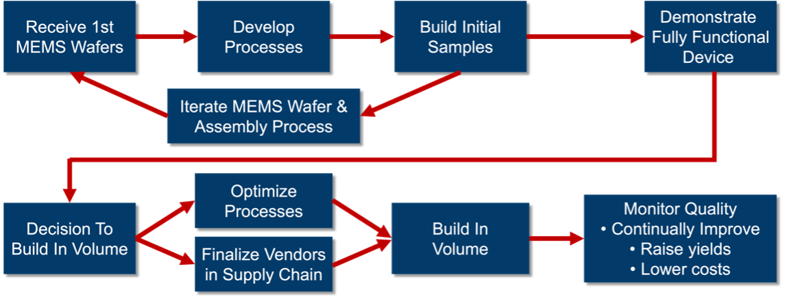
Figure 1 shows a typical project flow that would run through our operation. Ideally, once you obtain the MEMS wafers, you develop a process and build initial samples, and then the process gets integrated. However, the reality is that most MEMS devices are not finalized with the first wafer run. You may need to go through as many as half a dozen before you have a fully functional device. If, at this point, you decide to build in volume, then you focus on optimizing your process to reduce cost and maximize yield and reliability. In parallel with this effort, you’re typically finalizing the vendors for the supply chain. Then, you build it in volume, monitor quality over time using all the standard techniques, and work to raise yields and lower costs.
Potential MEMS Project Issues
A number of issues can arise that could impact your project. Fabrication cycles, as well as re-spin cycle, often take months, so one of the big issues in MEMS packaging, development and commercialization is overcoming these re-spin lifetimes. It takes careful design review upfront to minimize the likelihood of problems.
Next, to maximize the amount of data you get out of every run, you need to plan ahead and have tools and packages ready to go once you have a wafer run. It’s especially important to buy any custom tooling you need early because in the current environment, parts and tools are all lagging as lead times have grown quite long. It’s not uncommon to see 12- to 16-week delivery times now on parts, tools and epoxies.
One of the difficulties with the current lead times is that work tends to start and stop—you get a wafer run, you work diligently to evaluate it and come to some conclusions, you re-spin it… and then you have to wait for it to come out again. It’s difficult for an engineering team to have to deal with this and still manage the workload, so these flows are being outsourced to companies like Promex that have a variety of programs running in parallel. We can start and stop without creating a problem.
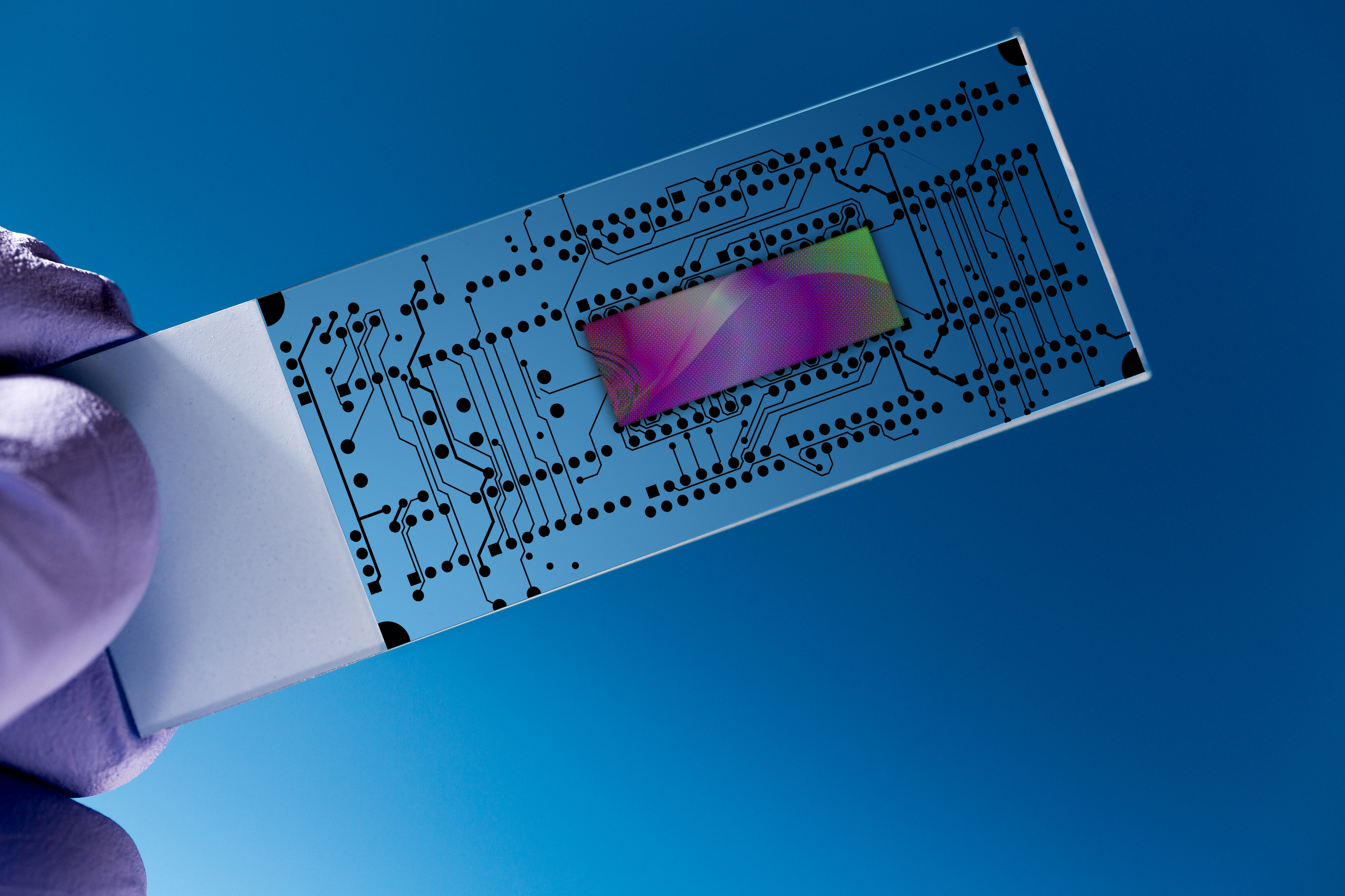
Because these projects can extend over a long period of time, maintaining accurate records is important, including taking photographs throughout the project life cycle. We photograph everything as we’re readying assembled MEMS devices for shipment.
Key MEMS Project Flow Considerations
We’ve identified three main areas to focus on when putting together your project flow. Going through these steps thoroughly will help ensure success and minimize problems.
#1: Choose your vendors carefully
Developing MEMS devices is a long-term program, so you need to ask some key questions to help you select vendors with whom you can develop lasting relationships:
- Do they have staying power?
- What’s their basic business strategy?
- What’s their historic performance with long-term projects? Do they have long-term customers?
- What are their internal controls or credentials?
- What’s their ownership approach? Fundamentally, ownership drives much of what a company does.
- How do they shorten your supply chain? You want to minimize the number of vendors in series, or even in parallel, as best you can, to minimize errors and maximize yields.
#2: Build initial samples manually
When you’re building one or two samples, they will be built manually, not by automatic machinery. Thus, you should be working with your vendors during the MEMS design phase to make sure that their capabilities are compatible with your design. Perform a thorough analysis of any vulnerabilities and/or issues with your device so that you can provide clear guidance and instructions to your vendors—particularly your assembly house—to prevent any misunderstandings.
It’s important that you train operators how to handle and process your unique device, making them aware of its fragility. They’ll need to take particular care with respect to susceptibility to scratching, particulates and other potential sources of damage, and you’ll want to ensure that they employ careful pick-and-place techniques. Make it a priority to meet with your assembly house on a quarterly basis to keep them up to speed on what’s most important in your device.
#3. Prepare for manufacturing
To prepare your device to manufacture in volume, ultimately, you’ll want to eliminate manual processes and use equipment placing as best you can. You’ll also want to implement good data acquisition methods that use today’s statistical process control (SPC) tools, which will help you maximize yields and quality. And you need to design and acquire early on the custom fixtures and packaging necessary to transport your device. As fragile as MEMS devices are, you can’t just pop them into a padded shipping envelope and expect them to reach their destination intact. Oftentimes, these devices require a carefully designed package to transport them safely from vendor to vendor.
Summary of Key Issues
Below is a condensed checklist of things to keep in mind with respect to determining your MEMS packaging and assembly approach. Following the guidelines we’ve provided in these two blog posts will help streamline your workflow and help you get your MEMS products to market on time, on budget and with all the functionality you need.
- Ensure your MEMS concept will work early
- Confirm that it meets the expected application requirements
- Minimize development time (and thus cost)
- Minimize the number of MEMS wafer fabrication cycles
- Maximize the info gained from each cycle
- Procure all custom tools and materials that MAY be needed; saves time upfront
- Minimize the piece/part cost, and design for manufacturing
- Start with hermetic to prove business model
- Move to organic to reduce manufacturing costs
- Minimize the supply chain depth
- Reduce number of sequential vendors
- Select stable vendors with solid credentials
Promex Industries’ Unique MEMS Offering
- Many process options from one on-shore source
- Headquartered in Santa Clara, California
- Stable, long-term supplier of assembly services
- Established in 1975
- Lengthy historical success
- 1000+ customers over last 10 years
- 100’s of projects taken from development to production
- Broad credentials
- ISO 9001:2016 – FDA compliant
- ISO 13485:2015 – ITAR registered
- FDB registered – Deep quality management system
When you’re ready to engage with a packaging and assembly provider, keep Promex in mind. Click here to contact us today.