
Part One
Microelectromechanical systems (MEMS) devices have become part of everyday life, as they are being incorporated into an increasingly wide range of applications, from smartphones to industrial instrumentation to medical devices to vehicles. In essence, the applications for these versatile devices are limited only by our imaginations.
As MEMS applications grow increasingly diverse, so do their individual requirements, such as requiring specific sensor types. Hardware is increasingly becoming a solution enabler, and this is putting even more stringent requirements on price, footprint and power consumption. This can lead to challenges when incorporating MEMS into products, as they possess unique characteristics that must be considered for assembly and packaging.
Two primary groups of challenges arise with respect to providing MEMS assembly services:
- Process flow – the MEMS assembly sequence implemented in the facility
- Project flow – long-term focus on everything that happens with a MEMS project
In this first installment of a two-part blog series, we will share Promex’s perspective on and approach to MEMS, and we will delve into a typical process flow. Part two will look at the key issues and considerations that must be taken into account when you create a project flow, as well as what a typical project flow looks like.
Evaluating Your Device
MEMS devices are essentially a subcategory of heterogenous integration. MEMS assembly and packaging have unique characteristics, which we’ll touch on as we go into the issues presented by the two types of flows.
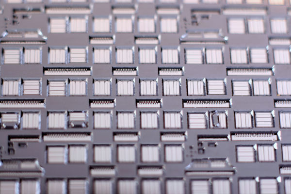
Before you can decide on the process or project flow, you must first evaluate the MEMS product: how big is the device, what are its characteristics, what metallurgies are on the surface, what are the wafer sizes and properties, including wafer thickness. Silicon wafers are made with standard thicknesses, ranging from 525 microns for 100mm wafers to 775 microns for 300mm wafers. While the MEMS die typically retain this thickness through the process, the wafers can be thinned as desired, but this must be done carefully to prevent damage.
After the evaluation, you select the MEMS package, develop and validate an assembly process, and, finally, go into volume manufacturing. This sounds straightforward, but package options vary greatly, depending on the properties and unique needs of the MEMS device.
Selecting Your MEMS Package
Figure 1 shows the range of package and lid types that are available from Promex—including plastic, ceramic and metal—as well as lid sealing, die attach and singulation options.
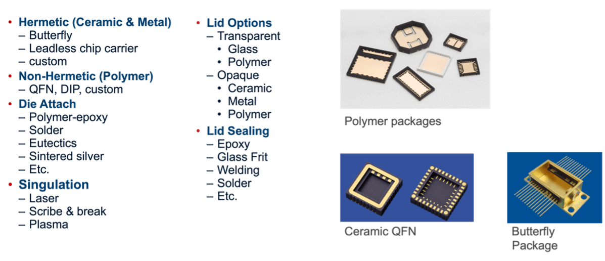
Figure 1. MEMS package options
MEMS generally are not overmolded; rather, they are inserted into a package with an air cavity surrounding them and a lid that can be attached using a variety of methods. For example, ceramic butterfly packages with glass lids are popular for MEMS because they are highly robust.
The two main types of packages are hermetic and nonhermetic. Hermetic packages are made from nonorganic materials (typically metal or ceramic) and are closed with an airtight seal that prevents moisture and contaminants from entering the package and damaging the device. Nonhermetic packages are typically made from organic, polymeric materials.
Hermetic packages are low-risk, stable and robust, but they’re expensive, with cost typically 10 times that of an organic package. Nonhermetic packages are much less costly, highly versatile and available in a wide range of materials. However, they require much more design work and testing, as they’re susceptible to many failure mechanisms that hermetic packages are not, such as gas and moisture permeation, adhesive bleed or shift, and recondensation. In many cases, you can use a hermetic package to prove that the MEMS concept works, and then convert to organic to lower the cost, when viable.
Developing Your Process Flow
Figure 2 illustrates the typical process flow that we implement. Once we get a MEMS wafer from a fab, we can implement a variety of processes, depending on what’s needed/appropriate. Then, we can build parts right on top of the wafer. We do this quite frequently; for example, we may receive a 12-inch wafer with MEMS devices fabricated on it, and we can add to it before singulating. With MEMS, laser singulation is typically used; saws require water, which can cause damage. That’s one of the choices to be made when selecting the assembly process. Then, as the illustration shows, the MEMS device is picked, epoxy or solder paste is applied, the device is placed and the electrical connections made—typically, using wirebonding—and the protective lid or cover is added (encapsulation is rarely used for MEMS). Once this process is complete, the device is final-tested, marked, documented and then shipped.
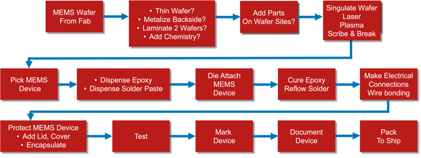
Figure 2. Typical MEMS assembly process flow
Handling during the assembly process is critical, as MEMS are fragile. They have micron-scale feature sizes, they undergo nanoscale movements and they are highly susceptible to scratching. This requires the use of specialized pick-and-place tools. Another variable to keep in mind is the potential for damage caused by reliability failure mechanisms such as electrostatic discharge, stiction or mechanical shock.
MEMS also require vigilance in keeping contaminant levels low. Particles most likely to incur damage in MEMS are those between 1-5 microns (or larger). Typically, packaging of semiconductor devices is performed in Class 10,000 cleanrooms, but those rated Class 100 or 1000 may be better options for MEMS assembly. This is another aspect to consider when creating your process flow.
The final two areas of consideration for process development are wafer singulation and die attach. As noted earlier, MEMS are typically singulated using dry lasers, but saws may be used for devices that are hermetically sealed or that can tolerate water. Plasma singulation is an emerging approach that uses reactive ion etching to cut. Its main advantage is that it doesn’t require straight cuts—it can cut in curves or unusual shapes, which we expect will be important for MEMS devices and the different kinds of applications they go into.
For the die attach method (Figure 3), there are a number of options to choose from, depending on your particular device requirements—conductivity, mechanical stability, thickness control, etc. Each of these considerations has its own potential impact. For example, if you use epoxy on an organic package, it’s important to monitor “bleed,” which is typical when they’re dispensed or when they sit around, and this can cause contamination. It’s also vital to use an appropriate curing technique. Epoxies and acrylates are commonly cured at room temperature or around 100°C, while some materials are cured for ultraviolet. If you use metallic attach, these materials require relatively high temperatures. Die attach film is rarely used for MEMS due to their inability to tolerate saw singulation. Finally, a customized pickup tool is important, as is monitoring the “keep out” or “no touch” areas to prevent damage.
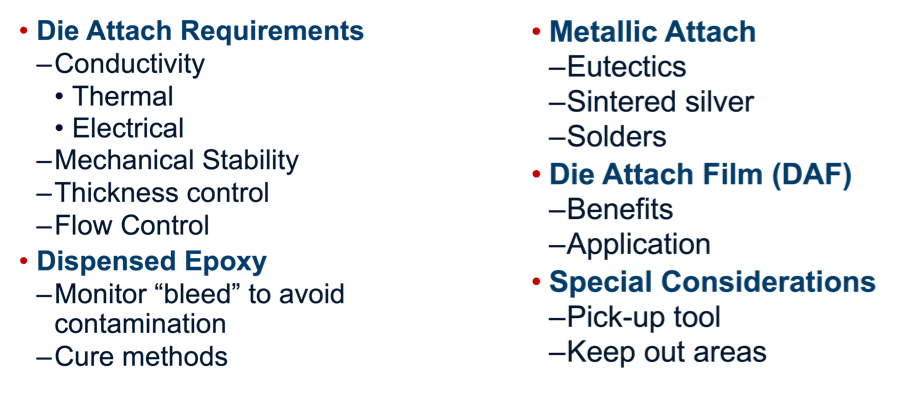
Figure 3. MEMS die attach requirements and methods
Once you have your MEMS device evaluated, your package chosen and your assembly process flow developed, it’s time to look at your project flow. Optimizing your MEMS project flow is essential to achieving reduced costs with high yields. We’ll explore this aspect in part two.