by Promex President and CEO Richard Otte
The increased functionality of today’s devices is mind-boggling. They go well beyond utilizing just electronics. Optical devices analyze chemicals, toxins, and biologic speciÂmens. Semiconductor devices control and switch kilowatts of power. MEMS devices utilize inertial methods to deterÂmine motion, direct light, and move comÂponents short distances. RF devices comÂmunicate wirelessly to other devices over the Internet. Even small acoustic devices like speakers and microphones that proÂcess sound are now used to gather and produce it. Devices go on and on, limited only by vision and technical cleverness to implement the visions.
To achieve this increased device functionality, a broad variety of dispaÂrate components must be combined. The challenges of this combining process – a.k.a. heterogeneous integration – are well known. However, increasing funcÂtionality also usually requires combinÂing devices with integrated electronics to process and analyze data gathered
by sensors, drive components that send information to users or other devices, store data and instructions, and more. Combining these disparate components with electronics requires an additional sophisticated process called heterogeÂneous assembly. Although it is not as widely discussed as heterogenous inteÂgration, it comes with just as many, if not more, challenges.
Heterogeneous Assembly Challenges
While mechanical assembly methÂods utilizing clips, screws, snaps, etc. are sometimes used for multifunctional devices, electronic methods (soldering, thermosonic metal-to-metal bonding, thermally and UV cured epoxies, acryÂlates, and other organics, etc.) are more advantageous. These methods take up a minimum of space, are compatible with most of the new heterogeneous compoÂnents, have low costs, are well develÂoped, widely understood, and readily available.
While electronic assembly is a good starting point, the specific and unique features of heterogeneous integrated devices often require improvements and modifications to the process such as:
- Reducing the temperature that compoÂnents are exposed to during the assemÂbly below the typical electronic range of 240°C to lower temperatures, someÂtimes as low as 40°C. This severely limits the number of electronic proÂcesses and materials and sometimes requires the development of new materials, joining methods, and equipment.
- Locating parts, such as optical fibers to lasers, with submicron accuracy and maintaining that location throughout the operating life of the device.
- Sealing interfaces to prevent liquids from leaking because the volume for analysis is small, or the liquid is poÂtentially harmful to the device, user or the environment.
- Modifying equipment, fixtures, and processes to build the product ecoÂnomically when the number of units to be built is small compared to the typiÂcal run quantity for electronic devices.
- Providing information systems to track, monitor, gather, store and report all of the information that highly funcÂtional devices require and produce.
- Building an assembly operation capÂable of running the increased number of processes often encountered when the number and variety of added comÂponents, along with their unique asÂsembly process requirements, are addÂed to conventional electronic methods.
- Unusual electrical requirements such as very high currents (hundreds of amps), very low currents (picoamps), very low voltages, or extreme elecÂtronic and noise minimization.
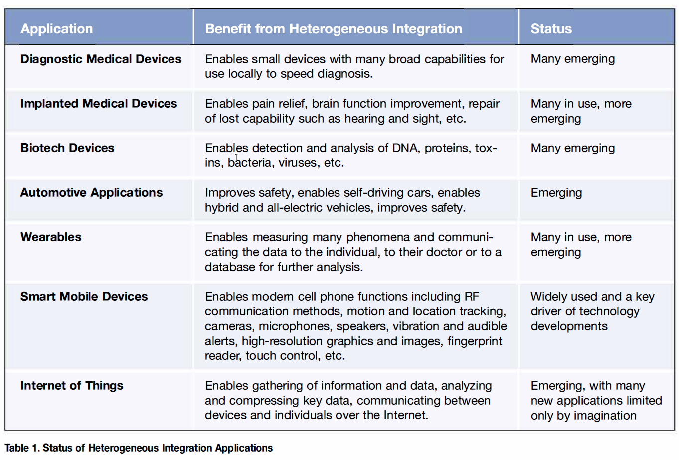
Table 1 lists some of the applications enabled with heterogeneous integration as well as their adoption status. Simply said, there is a lot of room for broader use.
Four Factors Affecting Heterogenous Packaging and Assembly
As with most products, good perforÂmance and low cost starts with and is dominated by good design. HeterogeÂneous integration makes the design funcÂtion much more complex than is typical for electronic products because many parameters can impact performance. Additional design issues include:
- Design software. Especially functionÂal simulation, as is done for electronics utilizing SPICE models. Models of that level of sophistication do not exist for most heterogeneous integratÂed products. Thermal and RF analysis is still being enhanced. Designing hetÂerogeneous devices often require the use of SolidWorks, 3D design and simulation software, as well as classic electronic design software, and usually some specialized custom software.
- The lack of good data on materials and their properties. This is a comÂmon issue for optical devices that require extreme mechanical stability to avoid unwanted optical effects over the life of a product. Optical attenuaÂtion results especially from thermal and stress-induced motion, but also from yellowing, crazing, etc. The RF properties of many materials (the dielectric constant and loss tangent) vary with frequency, water content, etc., in ways that are poorly documented. Medical and biotech devices in particular often directly come into contact with fluids or organic materiÂals that may either be contaminated by materials in the device or may cause the device to deteriorate in some manner. One extreme example is an implantable device where the materials that come into contact with tissue must cause no harm. Designing around the relevant detrimental phenomena is difÂficult even when material properties are well known.
- The availability of components and materials. Sourcing heterogeneous components are complex due to the wide variety of parts that must be sourced (Digikey will not stock everyÂthing!), the number of vendors needed, the length of the resulting supply chain, the cost resulting from margin stack from multiple vendors, and the need for some level of part traceability and compliance with the variety of quality requirements. Developing and managing the supply chain should begin with design and proceed in parÂallel. Good design is of no value if the parts, materials, and equipment requirÂed are not available in a timely manner with acceptable cost and quality.
- Cost. One of the most popular trends – the requirement to reduce the size of heterogeneous devices to make them more convenient to use, often minimizes power consumption and costs by utilizing a small amount of material. However, the cost is raised by the increased number of parts, the complexity of the supply chain, the number of assembly processes, and the increased precision required by the small size.
50+ Manufacturing Process Steps
As with the supply chain, heteroÂgeneous integration usually results in a greater number of assembly steps. At Promex, we find that it is not uncommon to need as many as 50 steps for heterogeneous assembly of a single device or product – sometimes even more.
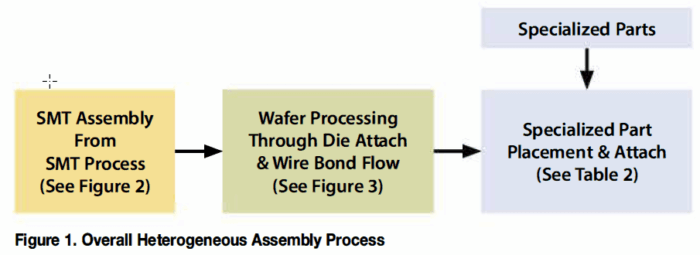
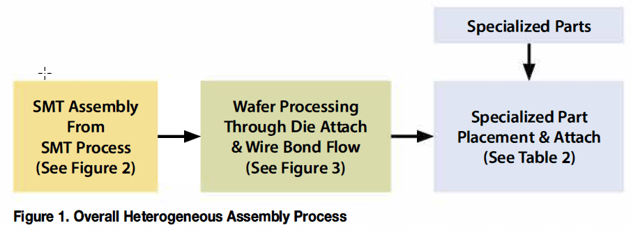
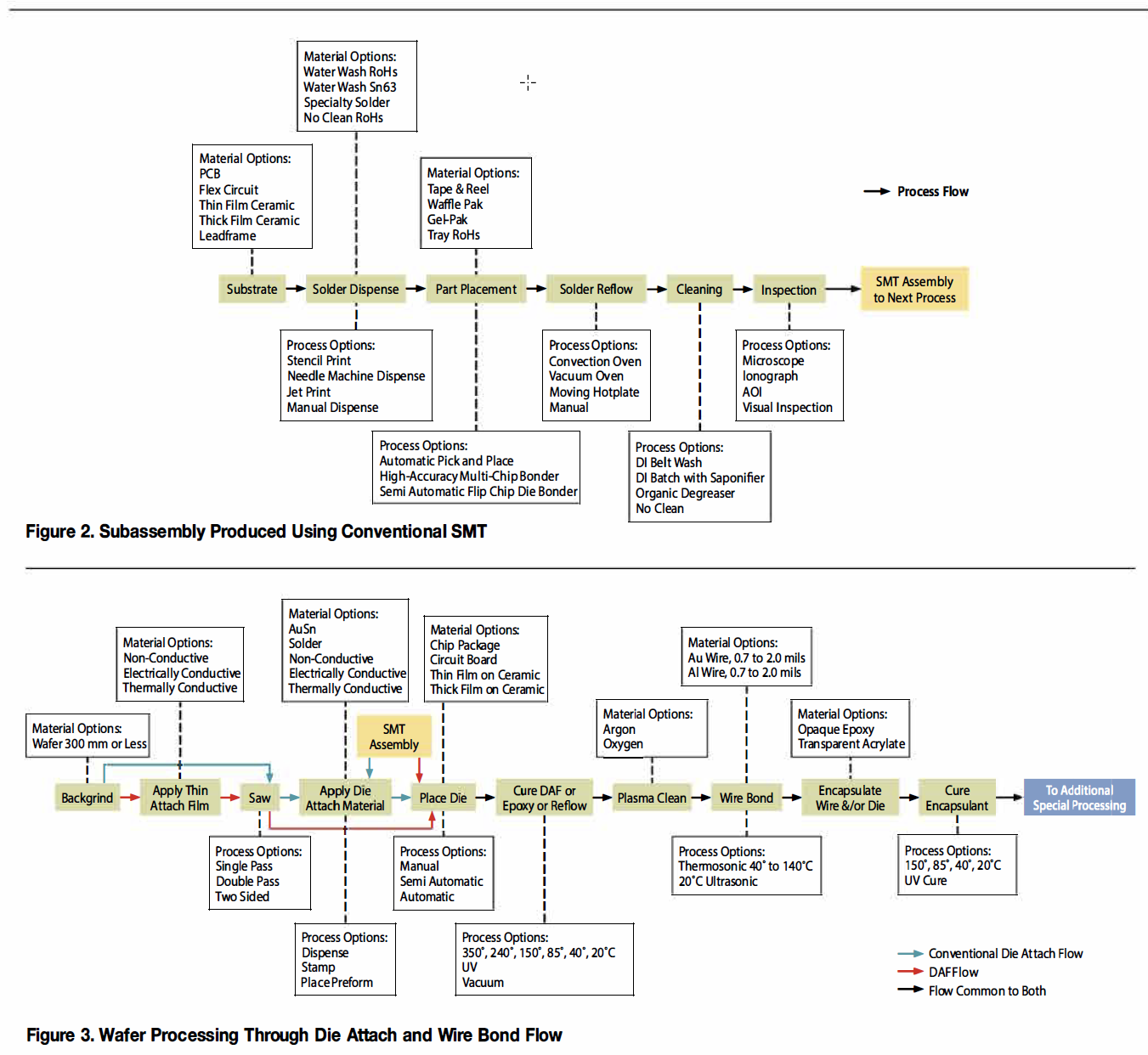
Figure 1 illustrates the overall heteroÂgeneous assembly process. Details of that process are shown in Figure 2, Figure 3, and Table 2. Assembly often starts with the conventional SMT process {Figure 2) that results in an SMT subassembly.
Figure 3 illustrates how the subassembly is often used as a platform on which die, which are often custom, are attached and connected.
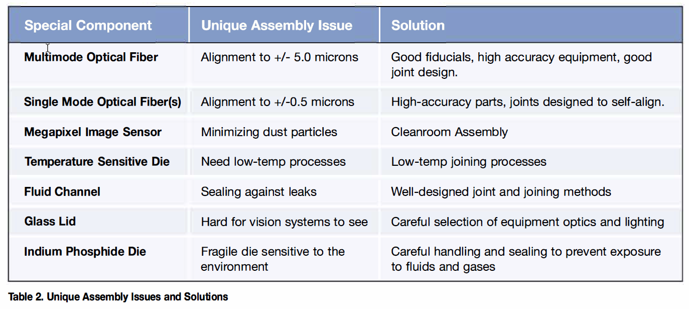
To build the final device, that subasÂsembly is then processed further with the addition of specialized parts using the appropriate processes. Table 2 provides examples of the unique assembly issues and solutions for a variety of special components.
In addition to the highly specialized processes in Table 2, more common packaging methods can also be utilized for heterogeneous devices, including:
- Die stacking with and without spacers
- Flip chip
- 2. 5 D integration utilizing Silicon interposer
- 3.0 D integration using through-silicon vias
- System in Package (SIP) utilizing mulÂtiple interconnected die and parts
While the assembly steps and packÂaging methods shown in Figures 2 and 3 are a good starting point, heterogeneous integration often requires combining these conventional processes with speÂcialized processes specific to the device. For example, while most electronic prodÂucts are built on printed circuit boards, many heterogeneously integrated devices are physically small and thus must utilize an equally small circuit board or other types of substrate. Substrate types include thick film ceramics, thin-film ceramics, silicon, glass, or flex circuits. Some of these are panelized, while others are provided as individual parts. Because processing multiple devices in parallel is a good way to reduce cost, substrates that are not panelized can often be placed in fixtures that not only enable parallel proÂcessing, but also minimize handling, or enable mechanizing of handling, and thus minimize damage during processing.
Summary
The global MEMS market is expected to reach an estimated $26.8 billion by 2022. Applications include the developÂment and increased use of smartphones and portable electronics, loT devices, RADAR/LIDAR, medical/biotech devicÂes with optical, chemical, RF, and liquid functionality, and electronic devices with increased interaction with the environÂment.
These new products combine mulÂtiple technologies with semiconductor technologies in a cost-effective way, ideÂally using a rapid process development cycle to minimize time to market thus enhancing market share and profitability. Combining the technologies requires improved design methods and software, more material properties, specialized manufacturing processes, and longer supÂply chains.
Despite the challenges, expect to see a greater number of products incorpoÂrating this philosophy due to the functionality that results from combining the data gathering, analysis, storage and communication capability of electronics with additional components that interact with the user and environment to gather information of all sorts and provide useÂful, often critical information back to the user.
Although there are still hurdles that must be overcome to cost-effectively build robust devices using heterogeneous assembly, experienced microelectronics assembly specialists such as Promex are putting all of their resources into overÂcoming those challenges.
For more information, contact DirecÂtor of Sales and Marketing Rosie Medina at 408-496-0222 or visit the Promex website at www.promex-ind.com.
Here’s a downloadable version (.pdf) of the presentation in the video:
Concept to Commercialization
Whether you need short-run proof-of-concept prototypes, high-volume production, or a second-source manufacturer, Promex can help. Reach out to us and let’s have a no-pressure conversation about how we might help advance your project to success.