A short video of how advances in semiconductor assembly and fabrication are re-shaping medical device design:
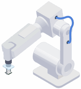
Advances in semiconductor assembly and fabrication are offering medical device designers new options for smaller, more compact, and more sophisticated designs. Often with onboard chips, rigid or flexible substrates and 3D stacked components. And there is often a requirement for integrated optical components and precision placement within plus or minus 5-microns in 3-axis. And the entire apparatus needs to be sterilizable and hermetic.
A recent project at Promex involved a new approach to endoscope design. In a traditional endoscope design, there is an optical chain that uses a series of optical elements; lenses, mirrors, image conduits, to carry the image from the lens to a camera or an optical eyepiece that the surgeon looks through to see what’s going on. So, you have a relatively large device with both a good deal of complexity and issues with the image quality where the surgeon is essentially working through the eyepiece of a microscope.
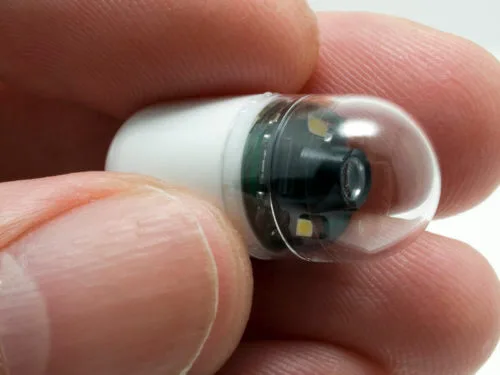
A customer came to us with a request to build an assembly that would replace this functionality with a miniature high definition, stereoscopic TV camera. Can we move the camera to the tip of the endoscope? This would create a sharper image, a simpler optical chain, and a device that would be smaller, thinner, and easier to handle.
So, such a device must have a series of unique characteristics. It must be able to be assembled and be very robust and take some amount of mechanical and physical abuse. And it needs to withstand sterilization.
This requires working through a portfolio of fabrication and assembly capabilities to develop the optimal approach to fabricate such a device. This required cGMP microelectronic manufacturing capabilities and Clean Room 100 facilities able to fabricate such a biocompatible MEMS assembly.
A key feature was the use of 3D assembly of the optical and semiconductor components into a stacked configuration to pack more function into a smaller space. A process using die attach film (DAF) and both precision flip-chip and wirebonding to create the final optoelectronic assembly to replace the older optical chain approach.
What we created was a 3D stacked camera assembly. There is a lens on top of the cover glass and an image sensor which along with the lens creates a miniature video camera. The entire assembly is just 8 millimeters across. An assembly with incredibly close dimensional tolerances that is the size of an eraser on the end of a pencil; forming a high-definition stereoscopic camera in full color. And the entire assembly is hermetically sealed and can withstand autoclave sterilization.
A successful design has got to work, must be robust, and must have good economics. And we are currently fabricating these units for the customer at our primary facility in Silicon Valley permitting a fully end-to-end onshore manufacturing in a one-stop-shop. Promex was able to take this project from prototype through to pilot production and then into full-scale production.
Here’s a downloadable version (.pdf) of the presentation in the video:
Concept to Commercialization
Whether you need short-run proof-of-concept prototypes, high-volume production, or a second-source manufacturer, Promex can help. Reach out to us and let’s have a no-pressure conversation about how we might help advance your project to success.