As medical treatments continue to evolve, innovation in medical devices plays a vital role, enabling increasingly complex, precise, and safer interventions. For example:
- Endoscopic devices provide high-resolution in vivo imaging,
- Wearable sensors offer real-time monitoring of vital signs,
- Implantable devices engage with the human body at the cellular level.
These devices’ ongoing advancements in reliability, accuracy, and miniaturization help to meet the ever-growing demands of modern healthcare.
However, successfully designing and manufacturing these devices presents significant challenges, especially for assembling complex sensors and microelectromechanical systems (MEMS) – a specific technology used to create miniaturized sensors and actuators by integrating mechanical components with electronic circuits on a single chip. Heterogeneous Integration (HI) has emerged as a transformative solution for these assemblies.


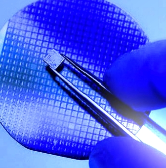
Heterogeneous integration starts with the full wafer (left) containing many individual dies (right). Each die then requires packaging to create the electrical and mechanical interconnections needed to be functional.
Heterogeneous Integration: A Revolutionary Approach to Microelectronics Assembly
Simply stated, HI is the process of assembling diverse electronic and non-electronic components into a single, compact device. This methodology, around which an entire industry roadmap has been built, emerged from three key technological advancements:
- Semiconductor innovations: New materials and advanced microfabrication techniques have enabled creation of smaller, more efficient components with enhanced capabilities.
- Global supply chains: Improvements in manufacturing and supply chain systems have made high-performance components more accessible than ever before.
- Advanced integration techniques: Wafer-level packaging, 3D integration, system-in-package (SiP), and other technologies have facilitated the creation of compact, high-performance devices.
These trends have paved the way for HI, which allows the integration of smaller, lighter, and more power-efficient components—such as sensors and MEMS—into devices that are computationally powerful but non-intrusive in size. Additionally, HI leads to more durable devices, as fewer external electrical and mechanical connections reduce the likelihood of failure.
Overcoming Design and Manufacturing Challenges of HI Sensors and MEMS
Despite its potential, HI presents unique challenges, particularly when integrating new components. While adding a sensor may enhance a device’s performance, it could also increase power consumption or complicate the assembly process. Moreover, to reach mass production, a device’s design must not only be optimized for functionality but also be scalable.
For a successful design, a thorough and structured development process is essential. Every aspect of the device—from design and component selection to manufacturing processes—should be considered holistically from the outset. This is where collaborating with the right Electronics Manufacturing Services (EMS) provider is crucial.
A qualified EMS partner brings critical expertise in managing complex integration projects. When evaluating EMS providers, it’s essential to look for credentials such as ISO 13485 certification, which ensures robust quality and risk management systems. Additionally, providers should have strong validation procedures, comprehensive operator training, and traceability for tools and parts.
At Promex, we combine industry-leading certifications with a proven process for transforming ideas into tangible products. We are ISO 9001:2016 and ISO 13485:2015 certified, and ITAR registered. Our engineers and designers leverage decades of experience and follow our Phase Gate Process, a structured approach that guides the design and manufacturing process from concept to production. This process defines manufacturing maturity at each stage, which enhances project predictability, reduces costs, and ensures that device method of manufacturing can be efficiently scaled for mass production.
To see the Phase Gate Process in action and learn how we have helped customers develop Lab-on-a-Chip (LoaC) devices – an impactful innovation in medical diagnostics – click here to download and explore our new white paper.