In Part 1 of this series, we explored the history of medical innovations and how new approaches, like heterogeneous integration (HI), are poised to enable groundbreaking new treatments. Here, we will expand on the role of HI, as well as the assembly challenges for these devices and the importance of working with the right partner to successfully bring new medical devices to market.
HI improves device functionality by expanding the types of parts and physical configurations that are combined with silicon chips. New different parts add new functions – often with minimal additional volume – thus increasing overall functionality per unit volume. By comparison, classic methods using packaged die employed to build electronic products, e.g., circuit boards or metal boxes, increase product volume, weight, etc.
Device additions via HI typically are physically small parts, features or coatings that are added to the silicon die or wafer. The electronics are built into the silicon wafer in the usual manner, with other parts added on the surface and combined so that electrical contact is made where needed. This approach to improve overall device functionality is not new. What is new is its increased appeal as the “path of least resistance” to increasing functionality per unit volume. Rather than implementing finer and finer lithography to make transistors smaller so that more are available per unit of wafer surface area, HI adds functionality vertically, utilizing a higher-level assembly such as a 2.5D or a 3D package.
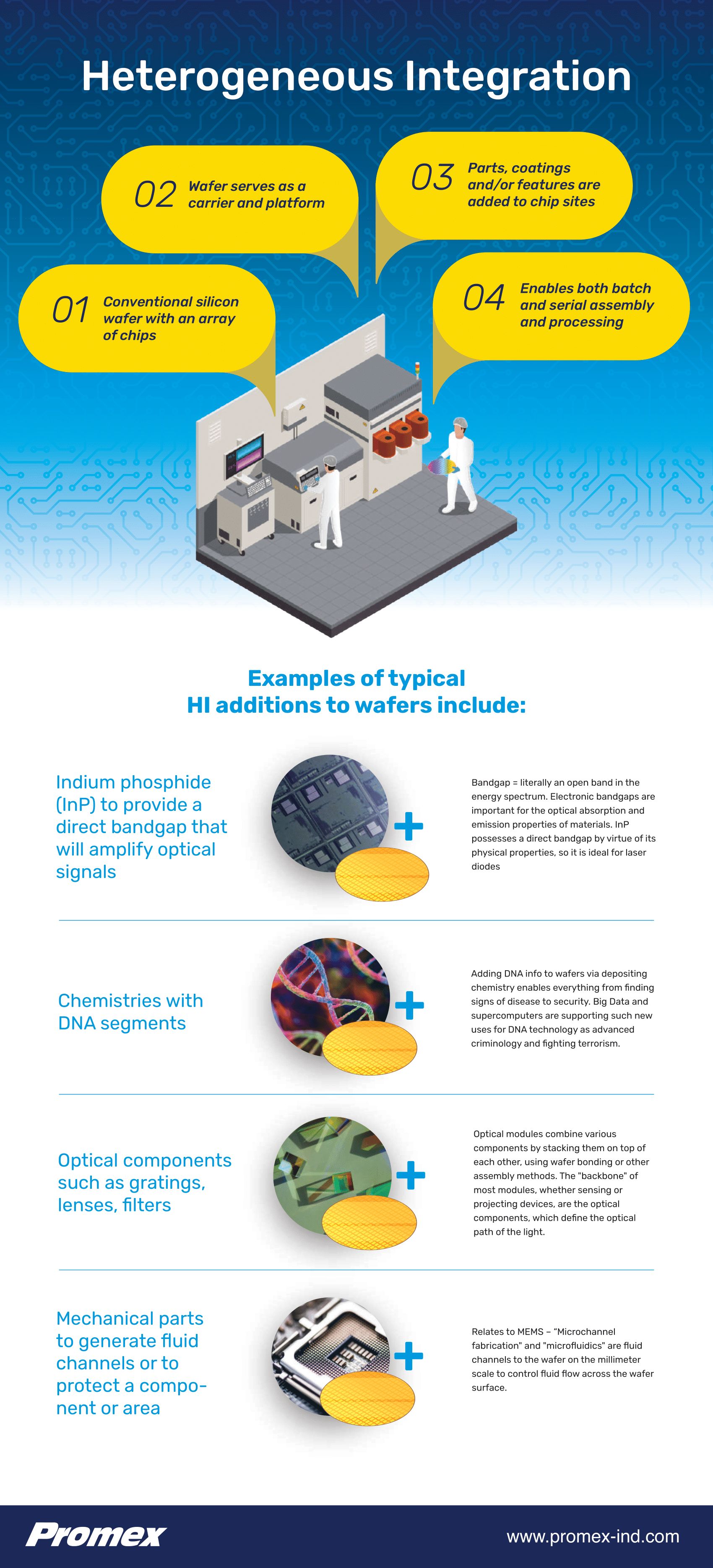
One HI approach utilizes a conventional silicon wafer with the usual series of chip sites. The wafer serves as a carrier and platform as parts, coatings and features are added to the individual sites. This enables both batch and serial assembly and processing.
Examples of typical HI additions to wafers include:
- Indium phosphide (InP) to provide a direct bandgap that will amplify optical signals
- Chemistries with DNA segments
- Optical components such as gratings, lenses, filters
- Mechanical parts to generate fluid channels or protect a component or area
After these additions, the wafer is singulated utilizing conventional processes such as sawing, laser dicing, or scribe-and-break. The result is a physically small, highly integrated device with significant functionality. It can be a finished, ready-to-use device; more commonly, it’s a component that will be mounted on a circuit board, substrate or subassembly that will then be combined with other parts to create a finished device.
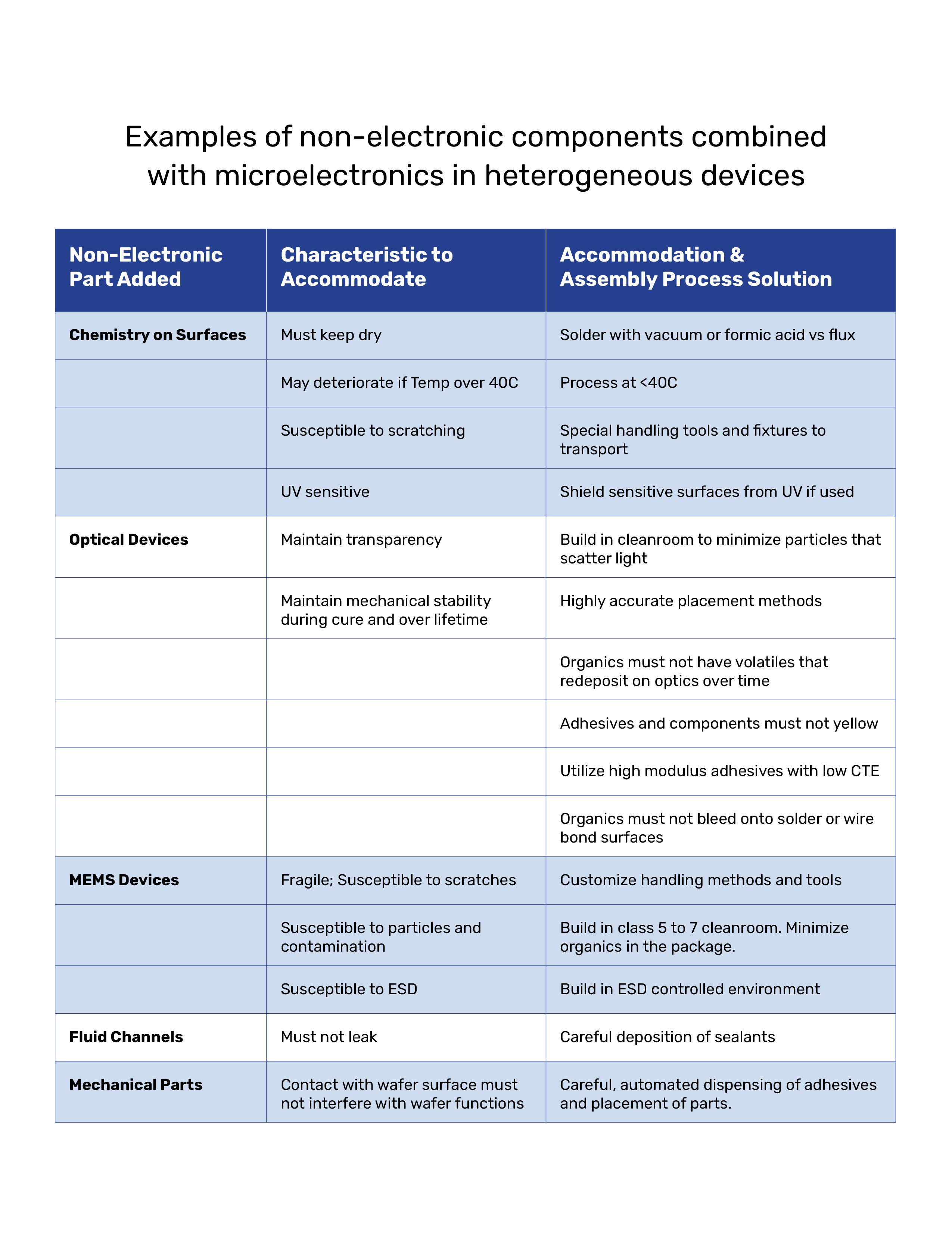
The assembly processes used to combine non-electronic and electronic parts must be customized to accommodate the non-electronic parts’ specific characteristics. The limitations imposed on the assembly process are highly varied and a function of the non-electronic parts. The following table lists some unique parts that may be combined with semiconductor die in heterogeneous assemblies, along with the characteristics that must be accommodated and the methods of doing so.
Promex specializes in developing customized assembly process needed to accommodate the characteristics of these unique component combinations. We have a variety of tools and processes available in one facility, with a dedicated engineering team, and this enables us to minimize both the development time and cycle time in production for our customers.