Heterogeneous integration (HI) has significant implications for the medical, health, and wearables industry. At Promex, we utilize a variety of complex assembly processes to achieve HI for medical and biotech applications. This post will take a closer look at the processes associated with assembling these classes of devices.
Figure 1 provides a high-level overview of our approach. Nearly every project these days incorporates some classic surface-mount technology (SMT) assembly to put standard parts on a circuit board, substrate, or flexible substrate. In the environment that we work in, many devices utilize bare die; so, with HI, we have the ability to start out with a wafer that comes out of a foundry and further process it – putting on die-attach materials, thinning it, sawing it, etc. We feed that into the later processes beyond conventional surface mount. In addition, in the medical and biotech devices that incorporate HI, there are almost always some unique specialized parts that have chemistries, optical characteristics, or specialized requirements of some sort that need to be accommodated in the assembly process.
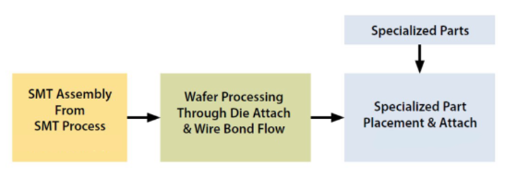
Figure 1. Generic heterogeneous process flow
The processes beyond surface mount are shown in Figure 2. We start with wafers that come out of fabs, we backgrind and saw them, and we may apply a die attach film (DAF) if appropriate. Then, we take a surface-mount assembly from our SMT process, and we place die, cure the attach materials, plasma clean the surfaces, create and encapsulate the wire bonds, and perform a final cure. Throughout this flow, as the figure illustrates, a wide variety of material and processing options are available to ensure that we can meet specific requirements for particular applications.
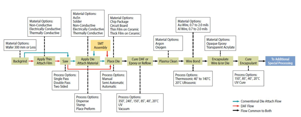
Figure 2. Conventional die attach on SMT subassembly
Finally, we come to the specialized processing that is truly unique to HI. Table 1 shows some of the specialized components that HI may require us to combine with conventional microelectronics and electronic assemblies. Each of these components often brings some unique requirements. Looking at how one can modify the processes to accommodate these challenges yields the solutions shown at right. Thus, each job that requires HI necessitates a careful analysis of the parts requirements and available capabilities to determine the best approach.
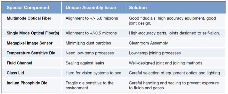
Table 1. HI solutions to specialized-component assembly challenges
Real-world examples
Figure 3 pictures some of the HI devices we’ve built over the past decades for medical, biotech, and other applications. To illustrate the scale of these minuscule parts, we’ve included a dime, which is about 18mm in diameter. At the upper left is an RF tissue marker for targeting cancer that’s injected using a hypodermic needle. The marker contains about 15 parts and is less than 1mm wide and 1.3mm in diameter. The device at the upper right is what we call a nine-die stack. It consists of three stacks of three die, with spacers between them, then “waterfall” wire-bonded to the substrate. This is technically on the edge of being an HI device, but it’s a fairly common assembly for us.
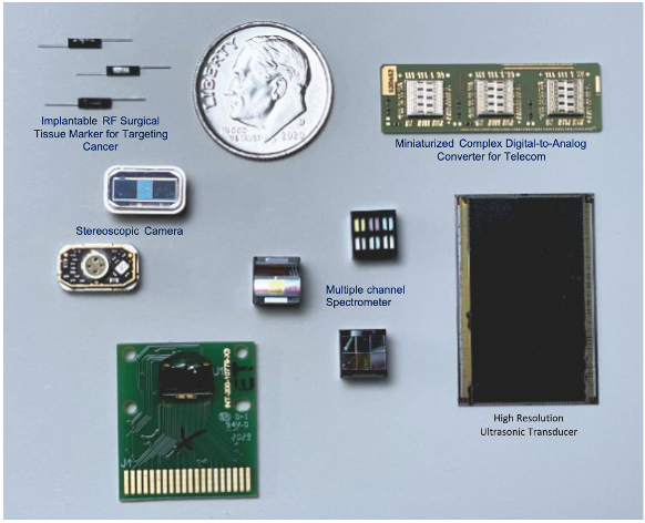
Figure 3. HI devices
The large device at the lower right is a microelectromechanical systems (MEMS) device interconnected to an application-specific integrated circuit (ASIC) with thousands of solder tip copper pillars; the ASIC is in turn mounted with DAF to a circuit board. The next three devices to the left, labeled “multiple-channel spectrometer,” are highly complex assemblies that incorporate tens of parts. In one case, these comprise LEDs, dichroic filters, optical channels, and, in the case of the detector, a lens, a series of other dichroic filters, and photodetectors. All these devices are part of an instrument that illuminates a sample that fluoresces when a pathogen is present that matches the chemistries hat have been introduced.
The lower-left device is a small circuit board containing a custom semiconductor device with chemistries on it that are susceptible to combinations of alleles, or gene variants, found in DNA. When a combination that’s appropriate for the chemistry is associated with it, the device gives out an electronic indication. The last two devices (middle, at far left) are two different sides of a stereoscopic camera used for endoscopic surgery. These cameras deliver high-definition stereo images. An optical chain goes on top of the upper version, and then we incorporate the whole thing, at a higher level, into a final subassembly.
These are just a few of the kinds of projects utilizing HI that Promex can help you develop, ensuring creation of a compact device that meets the needs of your medical, biotech, or wearable application.