By: Dick Otte, CEO of Promex Industries
As demand for higher-performance, more compact and energy-efficient electronics continues to escalate, traditional organic based substrates are approaching practical limitations, leading to industry experimentation with alternative materials. To this end, glass substrates have emerged as a promising alternative with distinct benefits for semiconductor packaging.
Major chipmakers, including Intel, AMD and Samsung, have development efforts focused on using glass or glass-core substrates for next-generation devices. While the rise of heterogeneous integration has created interest in introducing new kinds of materials and components for a range of applications, glass substrates raise packaging and assembly challenges that must be addressed.
First, why glass?
Glass is potentially an important material in electronic packaging due to its combination of strength and dielectric properties, which make it suitable for high-performance applications. Typically, electronic packaging materials such as glass epoxy with copper conductors are used in the industry. Glass provides some improvements over traditional epoxy in several ways.
The high modulus and high melting point of glass provides increased mechanical stability over a wider range of temperatures. In addition, applications requiring 1 gigahertz (GHz) clock speeds or higher, a low loss tangent (Df) reduces high-frequency signal component loss. This improves signal quality even though the propagation speed of signals is reduced somewhat by the higher dielectric constant of glass.
Table 1. Physical properties of substrate materials
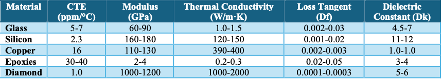
In summary, a major advantage of glass over epoxy is its ability to offer both strength and performance in high-frequency scenarios.
Available structures
While glass is a robust base material, it has limitations in terms of available structures and layers. Vias can be incorporated into glass, especially if the material is relatively thin – i.e., around 100 microns (µm)[1]. Both sides can then be metalized and patterned with conductors.
Additional conductor layers can be deposited and patterned on either or both sides if a suitable dielectric is used to isolate the added layers from the first and subsequent layers. While another layer of glass would create a consistent structure, deposition and patterning of the added glass layer is difficult. As a result, organic dielectrics, like epoxy, are commonly used as a secondary dielectric between conductor layers on a glass core. However, these organic materials tend to have higher loss tangents compared to glass. This makes them less optimal for high-frequency applications, where minimizing signal deterioration is important. Glass, therefore, remains an attractive option as the primary base material, with epoxy and other organic dielectrics playing a supporting role.
Application concepts
In recent years, the integration of optical waveguides into interposers has gained attention, particularly for emerging applications requiring high-speed data transmission. Glass offers the potential to fabricate low-loss single-mode optical waveguides within the glass core. One notable method for creating waveguides in glass is through laser-writing, a technique pioneered by Dr. Ben Yoo at UC Davis [2]. This innovation enables the fabrication of optical waveguides within glass substrates allowing for the integration of both electrical and optical components in a substrate and increases the functionality available to packaging designers.
Looking to the future, the physical volume occupied by a glass core might be replaced by a material or system to store energy to minimize time-dependent voltage fluctuations resulting from momentary variation in power demand. This might be accomplished by changing at least part of the glass core to a battery or capacitive energy storage material. An example of this type of approach was shared in the journal Batteries, published last year.
Another interesting material, and similar to glass in some ways, is diamond. Diamond has unusually high thermal conductivity that makes it attractive for applications with high thermal dissipation or that require uniform temperatures across the device, such as power and optical devices. The current high cost of diamond makes it financially viable only for small devices but that might change in the future. Glass, on the other hand, currently offers a balance between performance and cost, making it an appealing choice for a range of electronic applications.
What’s next?
Glass substrates open new possibilities for semiconductor packaging but require careful handling and innovative solutions to meet industry demands. While not yet positioned to replace epoxy entirely, they offer a valuable alternative for specific applications. As more companies invest in R&D to address manufacturing challenges, we can expect glass and glass-core substrates to play an important role in semiconductor packaging, particularly in high-frequency and high-density applications.
As a premier contract manufacturer specializing in intricate microelectronics component assembly, Promex can leverage our capabilities in a wide range of materials for packaging and assembly to help you optimize your device design. To learn more click here.
[1] See www.mosaicmicrosystems.com
[2] An example of the application of waveguides made in glass by laser can be seen in this video at the 2:45 mark: https://www.ucdavis.edu/news/uc-davis-photonics-technology-helps-shrink-telescopes