Die preparation is a vital step in semiconductor device manufacturing, comprising a series of precision processes that transform delicate wafers into reliable, high-yield dies ready for advanced packaging. At Promex, die preparation is a core strength of our packaging and assembly portfolio, ensuring the quality, yield, and reliability needed for mission-critical applications across medical, aerospace, defense, and other key end markets.
Each stage along the journey from wafer to packaged device demands expertise and control. Even minor errors can lead to device failures, yield loss, or reliability issues downstream. Tapping the capabilities of a proven leader like Promex for wafer thinning, dicing, sorting inspection, and die handling will allow your sensitive devices—whether based on silicon, compound semiconductors, MEMs or glass technologies—to meet the highest performance and quality standards.
Key Areas of Die Preparation at Promex
Wafer Thinning/Backgrinding
Promex employs advanced wafer thinning techniques, using precision backgrinding and finishing tools to reduce wafer thickness while maintaining structural integrity (Figure 1). This is essential for applications requiring ultra-thin profiles, such as stacked die assemblies, chip-on-flex, and chip-on-board (CoB) devices.
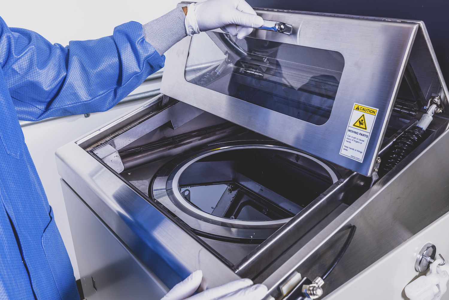
Figure 1. Laminated wafer ready for backgrinding
Our thinning equipment supports wafers up to 300 mm in diameter, achieving final thicknesses down to <25 µm with tight thickness tolerances and high accuracy (±5 µm). We work with you to customize the grind for your application based on the wafer material, topography, and desired roughness finish.
Tailored for silicon, glass, and compound semiconductors, our thinning process accommodates the latest package technologies and heterogeneous integration needs, and delivers an optimized surface finish for flatness, bondability, and minimal warpage.
Wafer Dicing
High-precision mechanical dicing is performed using industry-leading DISCO automated saws. The process is engineered for clean, accurate singulation with minimal chipping and tight dimensional control—crucial for today’s miniaturized and high-density devices.
As with thinning, our dicing systems support up to 300 mm wafers and offer dice-before-grind (DBG) for extremely small or fragile die. We can handle multi-project wafers and shuttle-run processing with ease, regardless of whether we’re working with silicon, glass, or ceramics.
Blade selection is a science at Promex: the team chooses the optimal blade material, thickness, and exposure based on the wafer’s material, thickness, layout, street width, and die aspect ratio. This ensures low mechanical stress, superior cleanliness, and maximum die yield.
Die Attach Film
Die attach film (DAF) is an essential process for applications requiring uniform die bond coverage and precise bondline thickness control. DAF is laminated to the wafer backside to serve as both the adherent material for the die and the support film (Figure 2). Following wafer dicing, die with DAF applied are picked off the support tape and placed on the substrate.
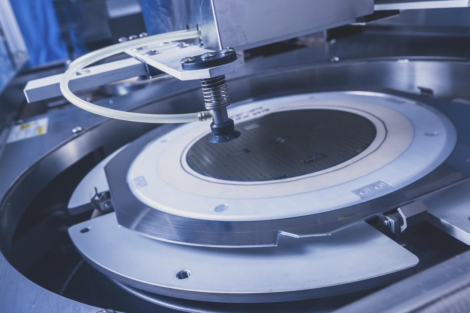
Figure 2. DAF-laminated wafer
By laminating wafers onto DAF prior to dicing, Promex ensures:
- 100% die attach coverage for stronger, void-free bonds
- Tightly controlled bondline thickness for optimal thermal and electrical performance
- Compatibility with high-density assemblies and advanced packaging formats
DAF is especially valuable for stacked die and heterogeneous integration applications, where die-to-substrate interface control is critical. Our process supports clean singulation of DAF-mounted wafers, preserving edge quality and minimizing handling damage during die pick.
Pick-and-Place/Die Sort
After the wafers have been thinned and diced (Figure 3), they are sorted using our high-accuracy pick-and-place systems. This is a crucial step to ensure that only functional chips are used in the next stages of manufacturing, making it key to yield optimization, quality control and cost reduction.

Figure 3. Diced wafer ready for pick-and-place
Promex can perform both manual and automated die picking. For automated picking, we can upload your electronic die sort map into the tool or use the tool’s optical vision system to select only known good die (KGD). We can also sort by die types, with full traceability to the wafer ID or die position.
The die sorter then picks and places the die into your preferred carrier, such as a waffle pack, Gel-Pak, or tape-and-ring—i.e., a reconstituted wafer. We can also leverage our partners to perform specialized picking from the diced tape to tape-and-reel packaging.
Die Inspection
Ensuring only KGD proceed to assembly is a Promex hallmark. Our trained technicians perform visual die inspection under a microscope, ensuring that the dies meet commercial standards or Mil-Std-883, Conditions A and B, or we can work with you to create a custom spec for unique device requirements.
Visual inspection of 100% of the die involves looking for minuscule defects such as chipping, broken traces, or bridging metal and segregating any damaged die from the visually good die. The primary benefits of this non-destructive inspection approach are enhanced defect detection, improved quality control, identification of subtle imperfections, and cost savings.
We specialize in handling thin and ultra-thin dies, and we can develop a custom workflow to meet your unique requirements.
What Sets Us Apart
- Experience with delicate high-value wafers – Promex has deep experience handling fragile materials and complex device designs, minimizing damage and maximizing yield.
- Tailored, customer-centric processes – Every project is approached collaboratively, with process parameters (like grind coarseness or blade type) determined in consultation with the customer to ensure the best fit for the application.
- Flexibility and turnkey support – We can process a wide range of wafer sizes, materials, and device types, offering turnkey solutions from wafer to package—all under one roof.
- State-of-the-art equipment – Leveraging industry-standard tools for grinding and dicing, and pick-and-place, Promex delivers repeatable, high-quality results to address your requirements, whether standard or highly specialized.
Die preparation is fundamental to producing reliable, high-performance microelectronics. At Promex, we execute every aspect with precision, expertise, and customer collaboration. Whether you need standalone die prep services or full turnkey manufacturing support, Promex delivers the quality and flexibility required for today’s most demanding applications.
Partner with Promex to smooth your devices’ journey from wafer to finished product—faster, safer, and with unmatched reliability.