
Artificial intelligence (AI) and high-performance computing (HPC) are pushing data infrastructure to its limits. As AI models become larger and more complex, the amount of data moving between processors, memory, and networking equipment continues to grow at an accelerating rate. The result is increasing pressure on system architects to find new ways to deliver higher bandwidth while controlling power consumption.
For decades, advances in electrical interconnect technology helped keep pace with performance demands. Today, however, those gains are becoming increasingly difficult to achieve. As data rates climb, electrical connections consume more power, generate more heat, and face signal integrity challenges that can limit overall system efficiency.
This reality is driving interest in co-packaged optics (CPO), an emerging approach that moves optical communication closer to the switching or compute die. While CPO has generated significant excitement across the industry, widespread adoption remains several years away. CPO holds tremendous promise, but important technical, manufacturing, and ecosystem challenges must still be addressed before it can scale to high-volume deployment.
Why Co-Packaged Optics Matters
Traditional data center architectures rely on pluggable optical transceivers located at the faceplate of a switch or server. Electrical signals must travel relatively long distances across the system before being converted to optical signals for transmission.
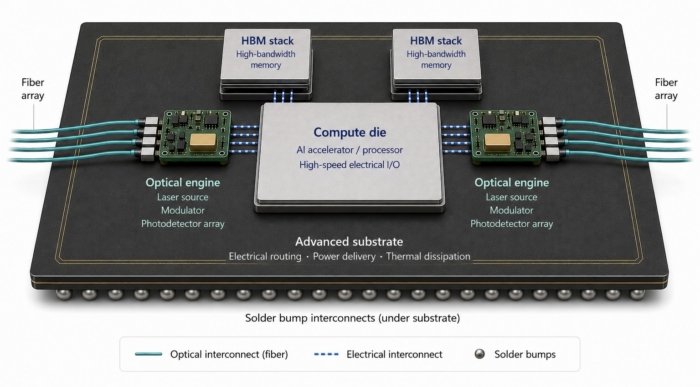
Co-packaged optics seeks to fundamentally change this model by integrating optical components much closer to processors, switches, and other high-performance devices. By shortening electrical pathways and enabling earlier optical conversion, CPO has the potential to reduce power consumption, improve signal integrity, and support the bandwidth requirements of next-generation AI infrastructure.
This approach is particularly attractive for hyperscale data centers, where power efficiency and performance directly affect operational costs and scalability. Industry leaders are actively investing in research and early deployments as they evaluate how optical integration can help address future networking bottlenecks.
At the same time, CPO is emerging alongside broader advances in heterogeneous integration, advanced substrates, hybrid bonding, and chiplet-based architectures. Together, these technologies represent a significant evolution in how complex electronic systems are designed and assembled.
Challenges Standing in the Way However, despite the momentum, co-packaged optics technology remains largely in the research, development, and early deployment phase. Significant barriers – described below and summarized in Table 1 – must be overcome before the technology can move from promising concept to mainstream manufacturing reality.
| Requirement for Mainstream Adoption | Current Status |
|---|---|
| Standardized architectures and interfaces | Still evolving |
| High-yield manufacturing processes | Under development |
| Cost-effective fiber-to-waveguide assembly | Early stage |
| Proven thermal management approaches | Active area of research |
| Mature design-for-manufacturing methodologies | Emerging |
| Broad supply chain participation | Limited today |
| Scalable advanced packaging infrastructure | Growing but not yet widespread |
| Electro-photonic component standards | Multiple proprietary approaches |
One of the most significant obstacles is the complexity of integrating electrical and optical technologies within a single package. Unlike traditional semiconductor packaging, CPO requires the precise interaction of electronic devices, photonic components, optical waveguides, fibers, thermal management systems, and advanced substrates.
These electro-optical interfaces introduce new design and manufacturing challenges. Multiple technologies that historically existed in separate domains must now function together within increasingly compact form factors. As more functionality is concentrated within the package, system complexity grows substantially.
Thermal management presents another major challenge. AI accelerators and networking devices generate considerable heat, often under highly dynamic workloads. Optical components, particularly lasers, require much tighter temperature control to maintain performance and reliability.
As a result, many industry experts currently believe lasers should remain separate from the primary compute environment to provide thermal isolation. This creates additional architectural considerations and increases the importance of co-design between packaging engineers, thermal specialists, and photonics developers.
Manufacturing readiness is another critical hurdle. Co-packaged optics introduces complex assembly processes involving precision alignment, optical coupling, and multi-domain integration. Each additional process step can affect yield, making manufacturability a central concern.
Design-for-manufacturing (DFM) methodologies for CPO continue to evolve, and the industry is still developing production-worthy process flows capable of delivering consistent, repeatable results at scale. Achieving high yields across complex assemblies will be essential for commercial viability.
The packaging infrastructure itself must also evolve. New methods are needed to efficiently transmit optical signals between front-panel connections and processors, memory, and networking devices. Meanwhile, increasingly demanding thermal requirements are driving interest in advanced cooling approaches, including greater use of liquid cooling technologies.
Material and substrate choices are also changing. Future CPO architectures may require broader adoption of silicon, silicon nitride, or glass-based interposers to support the integration density and performance requirements that next-generation systems demand.
Economic considerations add another layer of complexity. Developing new packaging technologies requires substantial investment, and much of today’s advanced integration capability remains concentrated among a relatively small number of leading-edge foundries and suppliers. In addition, high-volume optical module manufacturing is still heavily concentrated offshore, creating supply chain considerations for organizations seeking greater geographic diversification and resiliency.
Building the Path to Scaling
While the challenges are significant, none appear insurmountable. The industry’s history is filled with examples of breakthrough technologies that required years of ecosystem development before reaching widespread adoption.
Standardization will be a key enabler. As architectures mature, the industry will benefit from greater alignment around interfaces, integration approaches, and manufacturing practices. Clear standards can help reduce risk, accelerate innovation, broaden and simplify supply chains, and create more predictable pathways to commercialization.
Continued advances in photonics, electronics, materials science, and packaging technologies will also be required. Successful CPO deployment depends not on a single innovation, but on the coordinated evolution of multiple technologies working together.
Manufacturing readiness must advance in parallel. High-yield assembly processes, cost-effective fiber-to-waveguide integration techniques, and robust DFM practices will all play important roles in reducing costs and improving scalability. Process flows must be capable of delivering repeatable results while accommodating real-world manufacturing variation.
Equally important is ecosystem collaboration. Semiconductor companies, photonics developers, packaging providers, foundries, equipment suppliers, and hyperscale customers will need to work closely together to solve integration challenges and establish practical manufacturing models. Another factor to bear in mind is that CPO saves power but reduces flexibility in configuring the data center and makes the primary circuit board more complex. Table 2 highlights some of the practical issues associated with moving from faceplate transceivers to CPO.
| Utilizing Transceivers (TxRx) | Utilizing CPO | Benefit/Setback |
|---|---|---|
| High power consumption | Power reduced 25-60% overall by eliminating I2R and skin effect losses between faceplate and CPU/GPU/HBM | Increases power dissipated on the circuit board |
| Ability to choose/change TxRx range, wavelength, DSP, FEC and encryption | These functions must now be built into the main circuit board | Lose flexibility in configuring data center—cannot modify by changing TxRx so must change expensive circuit board |
| Laser/s are in the transceivers and hence replaceable | Must locate in temp-controlled location; should be pluggable, likely on the circuit board | An added design issue that needs to be addressed. |
| Optical fibers or waveguides are not needed on the main circuit board; only in the transceivers | Fibers or waveguides must connect faceplate to CPU/GPU/HBM and interface with optical modulators, lasers and detectors | Again, added technical issues that need to be addressed |
Notes:
- The circuit board contains CPU/GPU and high-bandwidth memory (HBM), hence is more expensive than transceivers
- Transceiver cost depends on range and “features” such as FEC, DSP, etc.
On the Horizon
Over the next five years, adoption is likely to occur gradually rather than through an immediate industry-wide transition. Hybrid electrical-optical architectures, such as near-package optics (NPO) may dominate during this period so some of the benefits of optical integration can be realized while the broader CPO ecosystem matures.
For advanced packaging providers and contract manufacturers, this evolution presents an important opportunity. Expertise in materials, substrates, precision assembly, thermal management, process integration, and manufacturability will remain essential as the industry works toward scalable solutions. Organizations that can help bridge the gap between innovation and production will play a critical role in transforming co-packaged optics from a promising concept into a mainstream technology.
The potential benefits of co-packaged optics are clear. The path to widespread adoption, however, will depend on the industry’s ability to solve the manufacturing, integration, and ecosystem challenges that stand between today’s prototypes and tomorrow’s production systems.
With more than 50 years of contract manufacturing and assembly under our belt, Promex stands ready to help you navigate the path from development to production for your CPO solution. Get connected with our team to learn more: https://promex-ind.com/contact-us/