Microelectronics Engineering Capabilities
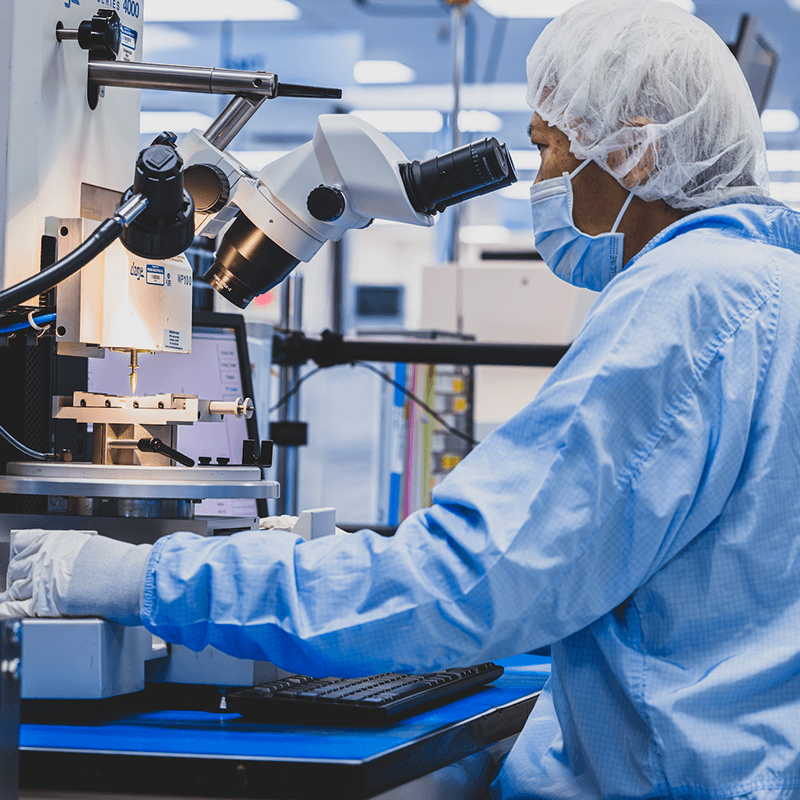
At Promex Industries, Inc. we specialize in advanced manufacturing design, packaging and assembly services for key subsystems that are used in a wide range of applications, such as diagnostics, life sciences, medical and MEMS devices. As a U.S.-based provider of advanced microelectronics assembly, including outsourced semiconductor assembly and test (OSAT) services, we are skilled at heterogeneous integration (HI) of tiny components with unique functionality and complex, custom or detailed assembly requirements.
Advanced Semiconductor Assembly Services
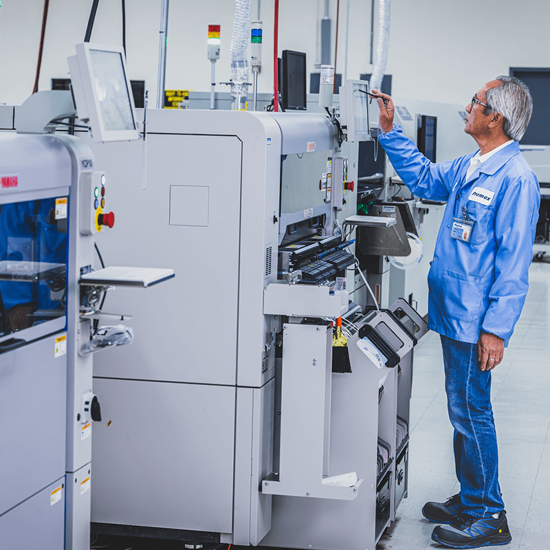
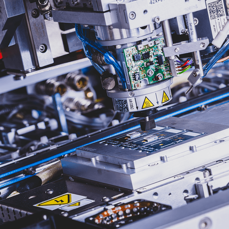
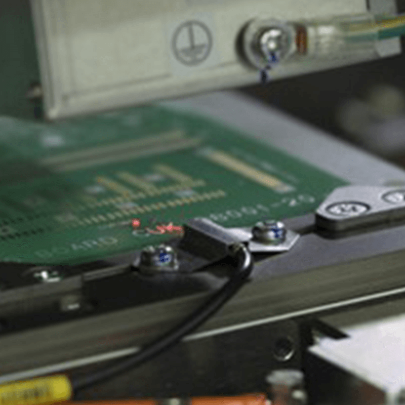
To produce these miniaturized devices, we combine multiple assembly technologies in a cost-effective way, using rapid manufacturing process development to minimize your time to market. During production, we ensure quality and consistent on-time delivery by collocating our services within one factory under a unified quality system. We implement sophisticated HI processes to ensure your complex device is manufactured through a well-optimized, repeatable process flow that expands what your device can do. Offering a range of semiconductor assembly services from SMT to module assembly, our services include: wafer thinning and dicing, die bonding, substrate design & fabrication, advanced packaging, flip chip assembly, and microelectronic integration. We provide end-to-end project management from development through production.
Heterogeneous Integration & High-Reliability Manufacturing
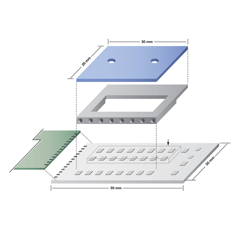
We develop customized process flows to assemble a mix of electronic parts and non-electronic parts without damaging the non-electronic items, such as optical components (including filters, lenses, and waveguides), piezoelectric devices, devices with on-board chemistry, fluid channels, devices with tight thermal restrictions, and other non-standard or specialized requirements.
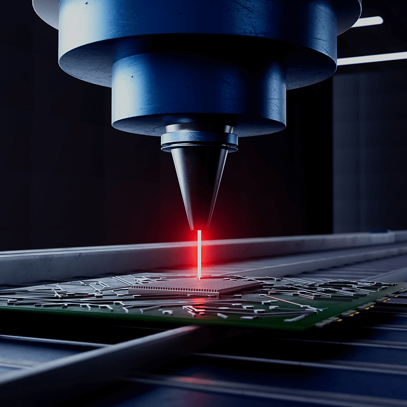
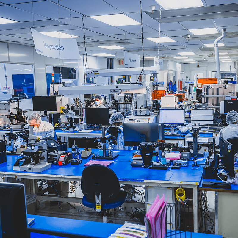
We maintain a broad variety of OSAT assembly tools and capabilities which we use to create robust assembly process flows. Our extensive metrology capabilities and technical expertise ensure requirement compliance throughout the manufacturing process and accelerates failure investigations.
Since 1975, Promex has served a variety of clients across the industries of medical & biotech, automotive, military and defense, data and telecom, and more. We operate a 30,000 sq-ft production facility, complete with ISO 5 & 6 (Class 100 & 1000) cleanrooms, and we are certified to ISO9001:2015 and ISO13485:2016. Our domestic manufacturing model provides customers with a flexible alternative to traditional offshore OSAT providers for complex, high-reliability applications.