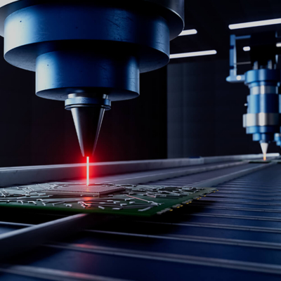
As advanced electronics continue to push the limits of materials, precision, and integration, laser processing has become a critical enabling technology. At Promex, laser micromachining and drilling are now part of our in-house manufacturing toolkit — supporting everything from delicate substrates to complex wafer-level applications.
To share further insight, we sat down with Jeff Schaefer, Senior Process Engineer and in-house laser expert, to talk about what Promex’s laser systems can do—and how customers are using them today.
Q: How long has Promex had laser capabilities in-house?
We’ve had our laser systems in operation for about a year now, supporting both development and production work. While laser is newer to Promex compared to some of our other processes, the team behind it brings decades of experience in packaging, assembly, and advanced manufacturing. That combination lets us apply laser processing in a very practical, production-focused way.
Q: What types of laser work does Promex currently support?
We do a lot of laser cutting across a wide range of materials, from flex and organics to more advanced substrates. We also perform laser drilling on both silicon and glass wafers. This flexibility is important because our customers are working with everything from traditional substrates to advanced materials used in next-generation packaging and integration.
Q: What role does laser processing play in PCB depanelization and custom geometries?
Depanelization is one of the primary applications for our laser systems. Laser cutting allows us to singulate PCBs and substrates quickly and with high precision, without introducing mechanical stress.
Because the process is non-contact, we can cut complex or non-traditional geometries that are difficult or impossible with mechanical routing — including circular boards, microSD form factors, and other custom shapes. This capability is especially valuable for advanced packaging designs where form factor and edge quality are critical.
Q: What makes laser processing valuable compared to traditional mechanical methods?
Because laser processing is non-contact, it allows us to work without applying mechanical force to the material. That means less stress, reduced risk of cracking or delamination, and much cleaner edges—especially on thin, delicate, or brittle materials. For many advanced devices, that difference is critical to long-term performance and reliability. Laser processing also complements traditional mechanical methods by its ability to cut practically any geometry that can be drawn in CAD, whereas traditional methods are typically limited to straight-line cuts.
Q: How does the Promex team approach new laser applications?
Every project is different. We always start by understanding what the customer is trying to accomplish, what materials they’re using, and what their performance requirements are. From there, we evaluate whether laser is the right tool — and if so, how to best apply it. It’s very much a collaborative, application-driven approach.
Q: How does Promex use laser processing to support tooling and production readiness?
One of the nice advantages of having laser processing in-house is how quickly we can respond to design changes or process needs. We routinely use the laser to fabricate or modify tooling, fixtures, and carriers used throughout assembly.
This allows us to make fast adjustments during development, improve process alignment, and reduce reliance on external tooling vendors. For customers, that means shorter lead times, fewer delays, and a more agile path from prototype to production.
Q: Can Promex support both prototyping and production with laser?
Yes — that’s one of the key advantages of having laser processing in-house. We can support early-stage development, prototyping, and scale-up to production without customers needing to shift between suppliers. That improves consistency, speeds up development cycles, and simplifies quality control.
Q: How does laser fit into Promex’s broader manufacturing capabilities?
Laser complements everything else we already do — from wafer prep and die attach to SMT, assembly, and final integration. Rather than treating laser as a standalone step, we integrate it directly into the overall manufacturing flow, giving customers a true end-to-end solution under one roof.
Q: What kinds of technical specifications should customers expect next?
As process development continues, we’ll be publishing more detailed laser specifications, including:
- Maximum material thickness for drilling and cutting
- Minimum and maximum hole/via diameters
- Supported materials (e.g., glass, silicon, ceramics, composites)
- Positional accuracy and tolerances
- Fiducial requirements critical for accurate laser alignment and repeatability
Q: What’s the biggest advantage for customers using Promex for laser work?
It really comes down to integration and expertise. Customers aren’t just gaining access to a laser tool — they’re getting the support of a full engineering, packaging, and manufacturing team that understands how laser fits into the entire product lifecycle.
Laser processing that supports next-gen design
With laser micromachining and drilling now part of our in-house capabilities, Promex continues to expand how we support advanced electronics, heterogeneous integration, and complex packaging challenges. Whether you’re enabling new materials, refining a precision process, or scaling into production, our laser team is ready to collaborate.