
Substrate Design & Fabrication
At Promex, we understand that the substrate is more than just a carrier—it’s the foundation of your microelectronic device’s performance. Substrate design and fabrication are critical components in semiconductor manufacturing, providing the foundational layer upon which electronic components and circuits are built. The substrate acts as a carrier, ensuring that all the tiny components within an integrated device are properly aligned and securely in place during the manufacturing process. Substrates can be made with various dielectric materials, including silicon, glass, and ceramics, depending on the specific application requirements. Conductors are usually copper, but other materials are possible.
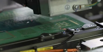
The fabrication process of an IC substrate involves several detailed steps. It begins with the selection of raw materials, followed by design and layout using CAD tools to specify dimensions, materials, and electrical pathways. The substrate then undergoes patterning and etching to create the necessary structures and interconnects. Various mechanical treatments are applied to ensure the substrate can support advanced integrated circuits. This intricate and precise procedure is essential for the performance and reliability of electronic devices, as substrates provide mechanical support, heat management, and electrical connectivity.
Promex offers custom substrate solutions for high-frequency and high-density applications. We can provide fully U.S.-based substrate fabrication, with a typical turnaround time of just 12 weeks. Our process includes designing substrates tailored to a selected fabricator, fabricating and electrically testing the substrates for accuracy, and assembling your die on the substrate. We have extensive experience with a variety of substrate technologies, including organic, ceramic, and flex substrates, as well as high-density interconnects and embedded passive integration.
Our substrate solutions support the broad range of markets, including medical, aerospace, defense, biotech, and advanced semiconductor applications. Whether you need a custom interposer, chip-on-board (COB) substrate, or fine-pitch flip chip-ready layout, we offer comprehensive design-to-delivery support.
Promex provides end-to-end solutions for your complex substrate interconnect needs. Our process includes:
- Collaborative substrate design – tailored to your application and compatible with selected fabrication partners
- Design-for-manufacturability (DFM) guidance – ensures smooth integration into the assembly process for a given fabrication partner
- Fabrication sourcing and management – using our trusted network of domestic and offshore partners
- Electrical testing – to verify signal integrity, continuity, and accuracy
- Die assembly and packaging – directly onto the custom substrate at our ISO 13485-certified facility
This integrated approach streamlines development, reduces risk, and shortens time to market – with typical turnaround times of just 12 weeks from design through fabrication.
Technical Details

Ceramic Design Rules
- In-house thick film ceramic substrate fabrication available for low cost and fast turnaround
- Lines and spaces to 15 µm/10 µm (thin film) and 100 µm/100 µm (thick film)
- Embedded passive components possible (thin film)
- Variety of plating options available, including patterned gold-tin (AuSn) solder and wire-bondable surfaces
- Several material options available: alumina, aluminum nitride, sapphire, and some optical glasses
- Material thickness from 127 µm – 1.27 mm
- Thin-film ceramic substrate design rules available upon request
Flex Design Rules
- Standard processing to lines/spaces 20 µm/20 µm
- Special processing to lines/spaces 1 µm/4 µm (2 layers only)
- High-reliability trace designs possible (> 50,000 bend cycles)
- Polyimide or liquid-crystal polymer (LCP) materials
- Stiffeners or rigid flex available
Glass Substrates
- Lines and spaces to <10 µm with through-glass vias (50 µm diameter) to accommodate high-density/performance interconnects and reliable assembly

Promex has longtime relationships with many of the most trusted partners in the substrate and fabrication market and can help you design, source, and manage fabrication for your custom substrate or interposer. Our substrate design and fab services are leveraged by a range of customers, including IC packaging firms, RF module makers, 5G network equipment providers, power device makers, implantable and other medical device companies, and manufacturers of high-rel solutions for military and aerospace applications—to name a few.
Additionally, our QP Technologies division designs substrates for a wide variety of chip packaging solutions.
From Wirebonding Inquiry to Full-Scale Production in Genomics
Turning a Sketch into a Production-Ready Module
