
Surface Mount Technology (SMT)
SMT Assembly Services
A key assembly method for placing and soldering microelectronic components onto printed circuit boards (PCBs) or other substrates, SMT revolutionized electronics manufacturing by allowing components to be mounted directly onto the surface of the board, as opposed to the traditional method of using through-hole technology to insert components. It optimizes space, speed, automation and precision, enabling advanced functionality and integration.
SMT is widely used in various industries, including consumer electronics, automotive, aerospace, telecommunications, medical devices, and industrial equipment. The technology enables the development of complex and high-performance electronic systems in a compact form factor.
Advantages of SMT
- Space efficiency: SMT allows for the placement of components on both sides of the PCB, leading to higher density and more compact designs. This is particularly important in miniaturized devices like smartphones and wearables.
- Performance and reliability: The direct attachment of components reduces the parasitic inductance and capacitance associated with through-hole components, improving electrical performance. Additionally, SMT components are generally more resistant to vibration and mechanical stress.
- Manufacturing speed: Automated machines can place thousands of components per hour with high precision, significantly speeding up the manufacturing process.
- Flexibility: The ability to mount components on both sides of the PCB and use a wide range of component sizes and shapes allows for more flexible and innovative designs.
- Cost-effectiveness: While the initial setup and equipment for SMT can be expensive, the reduced material costs, faster production times, and higher yields make it cost-effective in the long run.
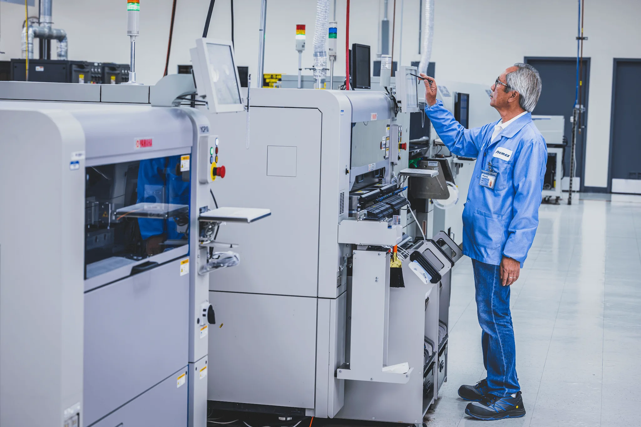
Promex delivers high-precision, high-reliability assembly for miniaturized components. With two full surface mount technology (SMT) lines, we offer both SMT-level and chip-level assembly under one roof—a competitive advantage unmatched in the industry.

One-Stop Shop for Assembly
Our broad range of SMT assembly services can accommodate:
- Fine-pitch and standard ball-grid-arrays (BGAs)
- Flexible and rigid-flex substrates
- A wide array of component sizes (including 008004)
- Chip-on-board (COB)
- Chip-scale packaging (CSP)
- Custom solder stencil and fixture design
- Components presented in multiple formats (including tape & reel, waffle packs, JEDEC trays)
- Nitrogen reflow
- Vacuum reflow
- Hand soldering
- Ball attach
- “Odd” form factors
- Singulation of panelized parts
- Variety of solder and reflow materials
- Device serialization
- True 3D solder paste inspection (SPI) system
Subassembly Using SMT Processes
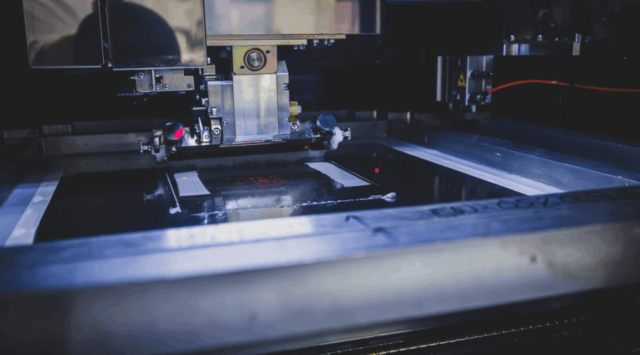
Our SMT subassembly process begins with the substrate, followed by solder dispensing, automated solder paste inspection, automated part placement, solder reflow, cleaning, and inspection. Collaborating with you, we select the best materials and processes for each step, ensuring precision and quality. We have some of the most experienced SMT operators in Silicon Valley and can guarantee extremely high quality for the most challenging projects and needs at both new product introduction (NPI) and volume stages.
Specialized Part Placement and Attachment
Whether your device needs to incorporate fluid seals, optical filters, image sensors, or microelectromechanical systems (MEMS), we handle specialized parts with tailored processes. Your project moves seamlessly from specialized part placement to final testing, ensuring an efficient path to market success. Specialized process and materials include:
- Controlled dispense of sealants
- Vision system able to “see” optically transparent parts
- Robust processes for tight tolerances, odd shape, strong joints
- Class 100 particle control
- Thermal hierarchy management
- Acrylates & silicones
Some examples of projects utilizing SMT techniques that customers have tapped Promex to complete include:
- A minuscule chip (4x8mm, roughly the size of a grain of rice) for an endoscope—employs a two-sided SMT assembly on a ceramic substrate
- Leadframe-based multi-die assembly of test system for a molecular diagnostics firm—uses SMT of assembled components into an FR4-based module
- Medical device for a life sciences R&D lab—implements double-sided SMT on a rigid/flex PCB
Automated Solder Paste Inspection (SPI)
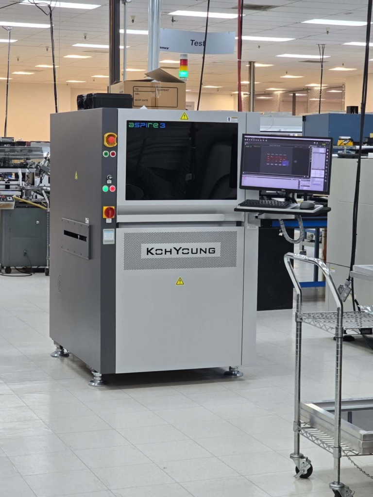
To meet the stringent demands of fine-pitch SMT, Promex has installed a Koh Young aSPIre 3 solder paste inspection (SPI) system—adding a brand new capability to our arsenal. SPI is used to evaluate the quality and accuracy of solder paste deposition on printed circuit boards (PCBs) during the SMT assembly process, ensuring proper solder joint formation and preventing defects.
Designed to perform 100% inline metrology, the aSPIre 3 system inspects solder paste deposits at every location on every panel—across rigid and flexible substrates—ensuring proper solder paste deposition. This system also captures detailed statistical data and builds optimal paste libraries for each design.
This data-driven approach delivers the highest standard in the True 3D SPI market, enhancing yield, enabling predictive quality control, and supporting tighter process windows essential to assembly of advanced components such as ball grid arrays (BGAs), chiplets, and high-density interconnects. These capabilities are especially critical for advanced assembly on thin, flexible circuit boards, where solder printing cannot be assumed to be consistent across the print area (as it would be for traditional, rigid circuit boards).

Additional benefits of SPI include:
- Improved yield and quality: By detecting defects early in the process — such as insufficient paste, excessive deposits, misalignments, or bridging — before components are placed, SPI helps prevent costly downstream rework and boosts first-pass yield.
- Process control and optimization: By continuously monitoring the solder paste printing process, our SPI system provides real-time data that can be used to adjust parameters, stabilizing the process and reducing variations.
- Defect reduction: A large percentage of PCB assembly defects originate from poor solder paste application; early inspection helps dramatically cut defects like opens, shorts, tombstoning, and poor wetting.
- Cost savings: Early defect detection saves money by reducing scrap, rework, and field failures. It also helps avoid more expensive repairs that would occur later in the line after component placement and reflow.
- Support for advanced technologies: SPI is essential for modern miniaturized electronics (e.g., 0201 passives, micro BGAs) in which solder volumes are minuscule and tolerances are tight. In particular, 3D SPI systems are valuable because they allow measurement of height, area, and volume, not just 2D coverage.
For your next project requiring SMT subassembly, Promex can help streamline development, integrating conventional SMT with our microelectronics packaging and assembly services to ensure you meet your time-to-market goals.
