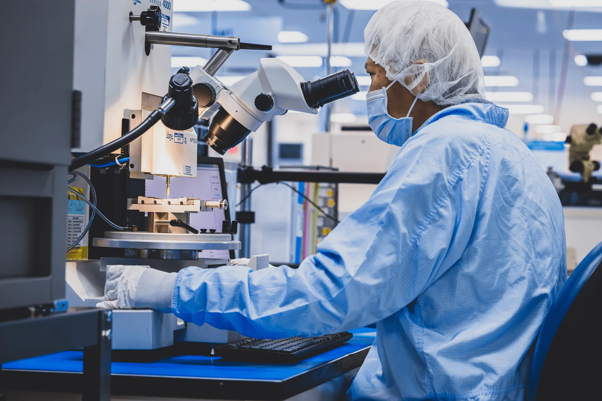

Metrology & Test
As semiconductor technology has evolved, the demand for smaller, faster, and more efficient electronic devices has driven the need for precise measurement and quality control. By identifying defects at an early stage, manufacturers can take corrective actions to improve production yield, reduce material waste, and ensure the reliability of semiconductor devices.
Metrology ensures the accuracy and precision of various manufacturing processes and entails using precise measurement techniques to ensure quality and accuracy of such critical parameters as dimensions, alignment, and material properties of the components and connections within a packaged semiconductor device. Metrology processes enable early detection of defects and optimization of manufacturing processes to achieve high yields and adhere to desired performance standards, and these measurements are crucial for maintaining the integrity and functionality of the devices–as even the slightest deviation can lead to performance issues, power inefficiencies, or even circuit failure.
In the era of the artificial intelligence (AI), high performance computing (HPC), internet of things (IoT) and big data, metrology and test are recognized as crucial processes that provide added value in hyper-scaling semiconductor manufacturing processes.
Promex’s robust inspection standards and quality control on incoming materials enable us to catch supply chain issues quickly and address them before they impact downstream yield.
Key Capabilities


- Optical inspection up to 300x enables us to maintain IPC610 standards, catch workmanship issues, and verify quality and cleanliness of assemblies. This capability is vital for SMT, sensitive components, optical assemblies like cameras, and particulate-sensitive assemblies like flow cells.
- Electrical and RF performance testing for high-power electronics and RF devices is key to optimizing and validating processes in the development stage and for verifying ongoing production quality
- X-ray imaging is used for in-process control on electrical assemblies and for damage-free inspection and analysis of semiconductor devices’ internal structures. The X-ray images aid in detecting electrical opens/shorts, and voids in solder and eutectic assembly processes, verifying the integrity of connections, and ensuring the overall quality of the semiconductor device.
- Confocal Scanning Acoustic Microsopy (CSAM) is used to non-destructively image material interfaces and discontinuities (voids/cracks) within a device.
- Automated X/Y microscopy moves the microscope stage in the X and Y directions, allowing for detailed examination of the wafer’s surface across a large area. Automation ensures consistent and accurate positioning—crucial for identifying defects, measuring dimensions, and ensuring the overall quality of the semiconductor devices. Cost-effective for process control and single-component tracking in both pre-production and production, automated microscopy is a critical part of all ongoing production programs at Promex.
- Destructive testing (e.g., wire pull, die shear, stud pull) is used in pre-production process verification to optimize and validate in-development processes and to verify ongoing production quality. This technology is particularly vital for high-reliability applications such as medical, aerospace, and telecommunications.
- 3D optical profilometry analyzes the surface topography of semiconductor wafers to provide detailed 3D images of device surface features. Used to control flatness of incoming materials and identify impact of assembly steps on part flatness, profilometry performs automated measurement of parts with non-planar geometry such as sensors—both large and thin single sensors and sensor arrays—and flex circuits for wearables and implantables.
- X-ray fluorescence (XRF) is a powerful analytical technique used in semiconductor manufacturing to verify metal stack-up on substrates and dies, is valuable for incoming quality control and process optimization.
- Laser interferometry verifies the flatness/thickness of components and adhesives at micron precision for multiple applications, including glass flowcells, and for small precision sensors.
- Customized product-specific test and measurement procedures. Promex can develop custom test methodologies for non-standard products or for heterogeneously integrated products with no readily available test methodology. We can also host and operate customer-developed test and measurement procedures in a production environment.
Customer Successes
Promex provides a range of metrology and test services for customers. Examples include:
- Taking over assembly from a customer that had been performing it in-house. Our in-process measurement enabled continual process improvement, which has led to the assembly yields increasing from <50% in-house to >99%.
- Performing inspection at every stage of assembly, as well as automated 3D measurement, test and/or buyoffs at critical-to-quality steps.
- Taking over assembly from a customer that had been performing it in-house. Our in-process measurement enabled continual process improvement, which has led to the assembly yields increasing from <50% in-house to >99%.

