
Laser Depaneling & Laser Micromachining
Promex has multiple in-house tools to perform laser singulation, micromachining, and cutting for a wide range of materials required for microelectronics and heterogenous integration. Our skilled staff can help you turn an idea into a reality, either as a standalone service or combined with other assembly services, simplifying your supply chain.
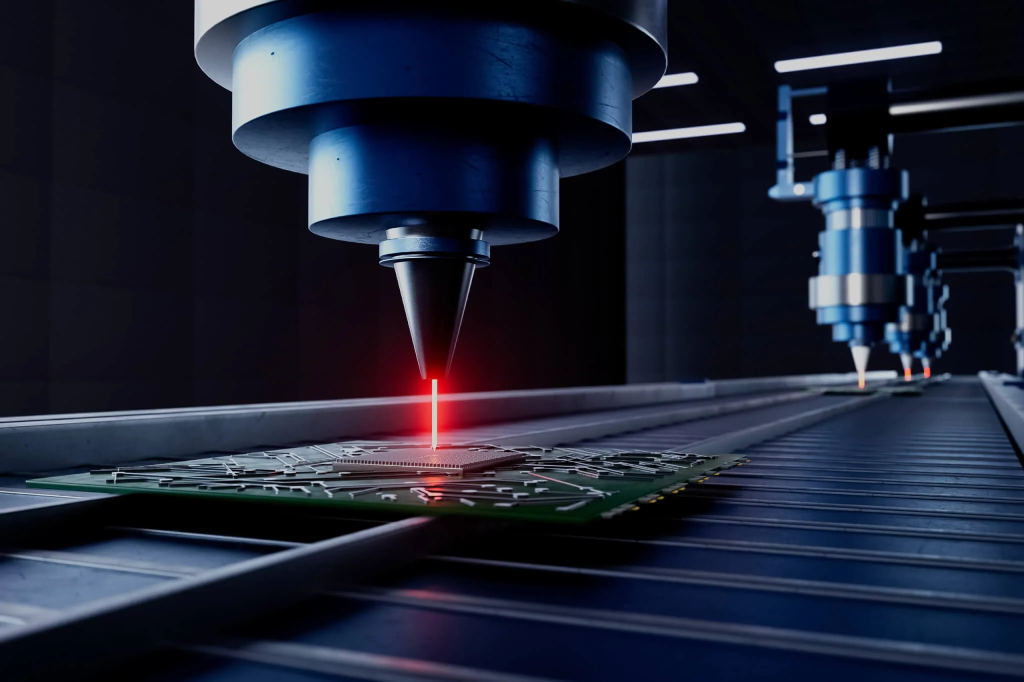
Laser depaneling uses a focused laser beam to separate individual PCBs from a larger panel after manufacturing. Widely used in PCB manufacturing, flex circuit depaneling, and rigid-flex board processing, the highly precise process minimizes dust and mechanical stress.

We feature an LPKF CuttingMaster 2127 (27W, 355 nm nanosecond pulse) laser with a spot size of <20 µm. This laser is ideal for cleanly and quickly cutting organic materials without melting, charring, or thermal stress, such as:
- FR4 circuit boards
- Polyimide flex boards
- Liquid crystal polymer (LCP) flex boards
- Organic/laminate substrates and interposers
- Overmolded components and other plastics/composites
With this tool, we offer the following prototype and volume production services:
- Circuit board depanelization (max. panel; thickness up to 2.0 mm)
- Maximum panel size: 350 mm x 350 mm
- Thickness range: Up to 1.6 mm (thicker upon request)
- Positional accuracy +/- 25 µm
- Allowed components within 30 µm of PCB edge possible
- Panelization layout design – can accommodate both AutoCAD (.dxf or .dwg) and Gerber (.gbr) files
- Save up to 30% dead space between devices on panel due to small laser spot size
- Laser drilling
- Laser circuit rework (trace cutting, solder mask removal)
- Board or device serialization
- 1D or 2D barcodes (data matrix, QR codes)
- Numerical serialization
- Logos or other artwork
- Process development and material cutting feasibility studies
Enabling clean, stress-free singulation of flex and rigid-flex circuits is key to meeting customer demand for chip-on-flex and flexible packaging solutions. Offering this capability in-house allows Promex to improve turnaround times, enhance process control, and ensure consistent quality for critical applications.

Laser Machining & Micromachining
Laser machining is a broader term that encompasses various laser-based material processing techniques. For other micromachining services, we have an ESI 5220 Laser Processing System that allows us to process:
- Glass and other optical materials, including sapphire
- Ceramics
- Silicon, including wafers
- Metals, including copper, nitinol, and stainless steel
Laser micromachining with this tool can accommodate parts up to 533 mm x 635 mm in size (thickness is material dependent), enabling:
- Silicon wafer coring from wafers up to 300 mm custom extraction of smaller development wafers
- Drill micro-vias as small as 25 µm in diameter
- Cut grooves, steps, channels, slots or cavities
- Inscribe alphanumeric characters, logos, or alignment features
- Trim, drill and dice MEMS devices
- Drill precision alignment holes
- Laser-cut stencils
- Cutting and depanelization
From Wirebonding Inquiry to Full-Scale Production in Genomics
Turning a Sketch into a Production-Ready Module
