
Heterogeneous Integration
Complex Assembly & 3D Integration Services
At Promex, we define heterogeneous integration (HI) as the process of combining diverse, separately manufactured components, often with different functionalities and fabrication processes, into a single, higher-level assembly, such as a system-in-package (SiP). This integration of electronic and non-electronic content within one compact package enables enhanced functionality and performance. Essentially, it involves integrating diverse components to create a more complex system by adding features or functionalities that can’t be achieved with just a single chip.
We make use of a range of complex processes to achieve HI for target applications. Nearly every project now incorporates some classic surface-mount technology (SMT) assembly to put standard parts on a circuit board, substrate, or flexible substrate.
HI expands function, not form factor
Common to many devices that incorporate HI is the inclusion of unique, specialized parts that have chemistries, optical characteristics, or other specialized requirements that the assembly process must accommodate. HI improves device functionality by expanding the types of parts and physical configurations combined with silicon chips. The electronics are built into the silicon wafer in the usual manner, with other parts added on the surface and combined so that electrical contact is made where needed. These different parts add new functions, yet very little additional volume, resulting in increased overall functionality per unit volume.
HI doesn’t mean reinventing the wheel. Many of the tools and techniques used in traditional electronics manufacturing—like SMT, printed circuit boards (PCBs), and flexible circuitry—are fully compatible with HI.
HI also supports 3D integration, allowing:
- Die stacking
- Use of ultra-thin die
- Embedding die in substrates
- Flexible substrates
This 3D capability increases density while minimizing the physical size and volume of devices resulting in a compact footprint, ideal for next-gen, miniaturized systems.
A key trend related to HI is the rise of chiplets. Chiplets are assembled using smaller, individual known-good die (KGD) and the fabrication technology that works best for each die. This is very different from a monolithic approach, where all functionality is integrated at a large die level using the most advanced fabrication node needed for the most demanding function within the device. This allows chiplets to deliver overall yield and cost improvements.
Different semiconductor types can be used depending on the application, e.g.: CMOS devices for general-purpose logic and memory; gallium arsenide (GaAs) or gallium nitride (GaN) for high-frequency RF; and indium phosphide (InP) or silicon carbide (SiC) for power or photonics. This flexibility ensures the best available technology is used for each function within the system.
The Heterogeneous Integration Roadmap was launched in 2016 as the successor to the International Technology Roadmap for Semiconductors. Some key packaging challenges being addressed by the current version of the roadmap include:
- Substrates for very large packages
- Reliability issues for advanced packaging
- Chip-package interaction at smaller nodes
- Materials for 3D printing
- Board-level power integration
- Adding to the classical electromigration model
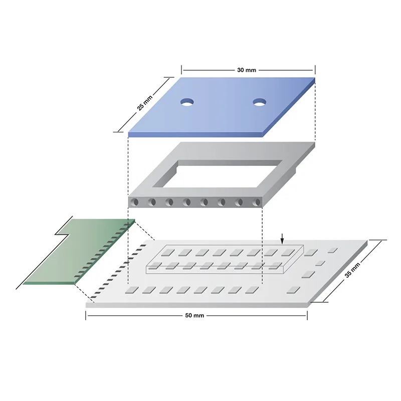
One HI approach utilizes a conventional silicon wafer with the usual series of chip sites. The wafer serves as a carrier and platform as parts, coatings and features are added to the individual sites. This enables both batch and serial assembly and processing.
Once these additions are complete, the wafer is diced using conventional processes such as sawing, laser, or scribe-and-break. The result is a physically small, highly integrated device with significant functionality. While it can be a finished, ready-to-use device, it’s more commonly a component that will be mounted on a circuit board, substrate or subassembly that will then be combined with other parts to create a finished device.
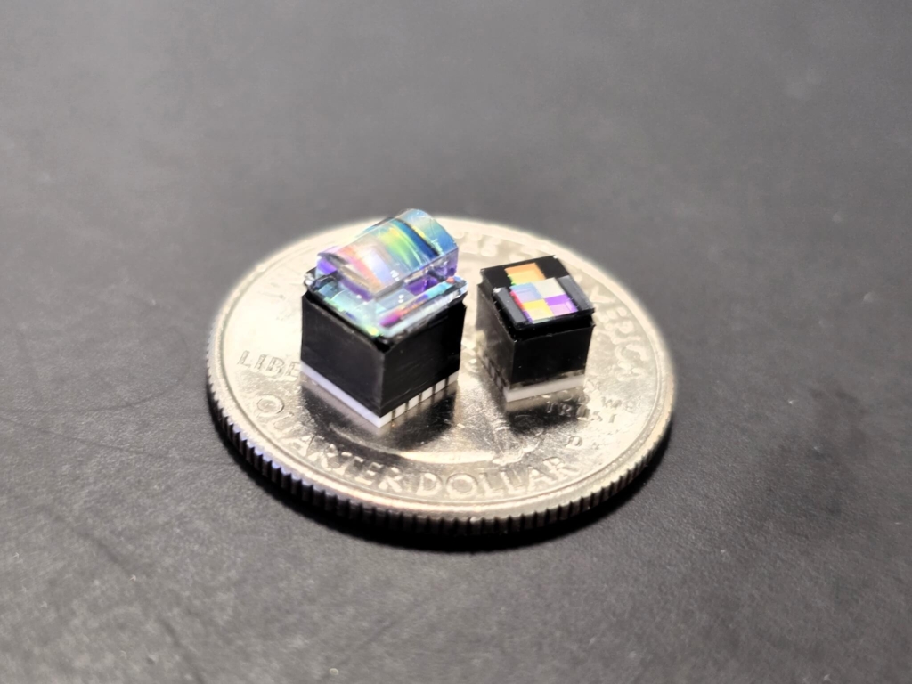
Promex is well-versed in these processes – we’ve been doing heterogeneous assembly for more than two decades. HI is already powering groundbreaking devices across industries. Examples include:
- Eye-implantable glaucoma sensor: A miniaturized sensor to monitor intraocular pressure
- 10-channel fluorescence spectrometer: Portable diagnostics with integrated optics and electronics
- Bio cartridge: Combines fluid handling, sensors, and data processing for point-of-care testing
- Smart micro SD memory card: Embedded with environmental sensors and on-board processing
HI is revolutionizing how we think about device design. By breaking down the barriers between materials, form factors, and functions, HI lets Promex build smarter, smaller, and more capable systems. Whether it’s a wearable sensor, a biomedical implant, or a next-gen communication module, HI makes it possible.
