
Wafer Dicing, Grinding and Die Preparation
Promex’s expertise extends to our full suite of die preparation services designed to support successfully transitioning semiconductor wafers into high-performance packaged devices. These capabilities include precision wafer thinning, dicing, die inspection, and die handling—all performed under tightly controlled conditions to ensure quality and repeatability.
Whether you’re working with silicon, compound semiconductors, or advanced substrates, our experienced team and specialized equipment are ready to meet the needs of complex microelectronic assemblies. Promex supports a wide range of packaging workflows, including chip-on-flex, chip-on-board, rigid-flex, and heterogeneous integration.
With a focus on yield, cleanliness, and dimensional control, our die prep services are tailored to serve high-reliability applications in medical, aerospace, defense, and advanced semiconductor markets.
Wafer Backgrinding
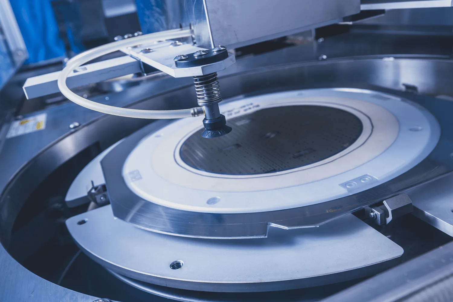
Our wafer-thinning process uses precision backgrinding and cleaning techniques to reduce wafer thickness while preserving structural integrity. This fabrication step involves thinning wafers down to 20μm to accommodate the latest package technology and stacked die applications. The process comprises several steps, including wafer mounting, grinding wheel selection, and optimization of grinding parameters. Automatic DISCO grinding equipment and supporting metrology tools, are used to ensure precision and accuracy throughout the process.
- Supported wafer sizes: Up to 300 mm
- Final thickness range: 20 µm to standard thicknesses
- Thickness tolerance: ±5 µm
- Surface finish: Optimized for flatness, bondability, and low warpage
- Materials supported: Silicon, glasses, ceramics, and compound semiconductors
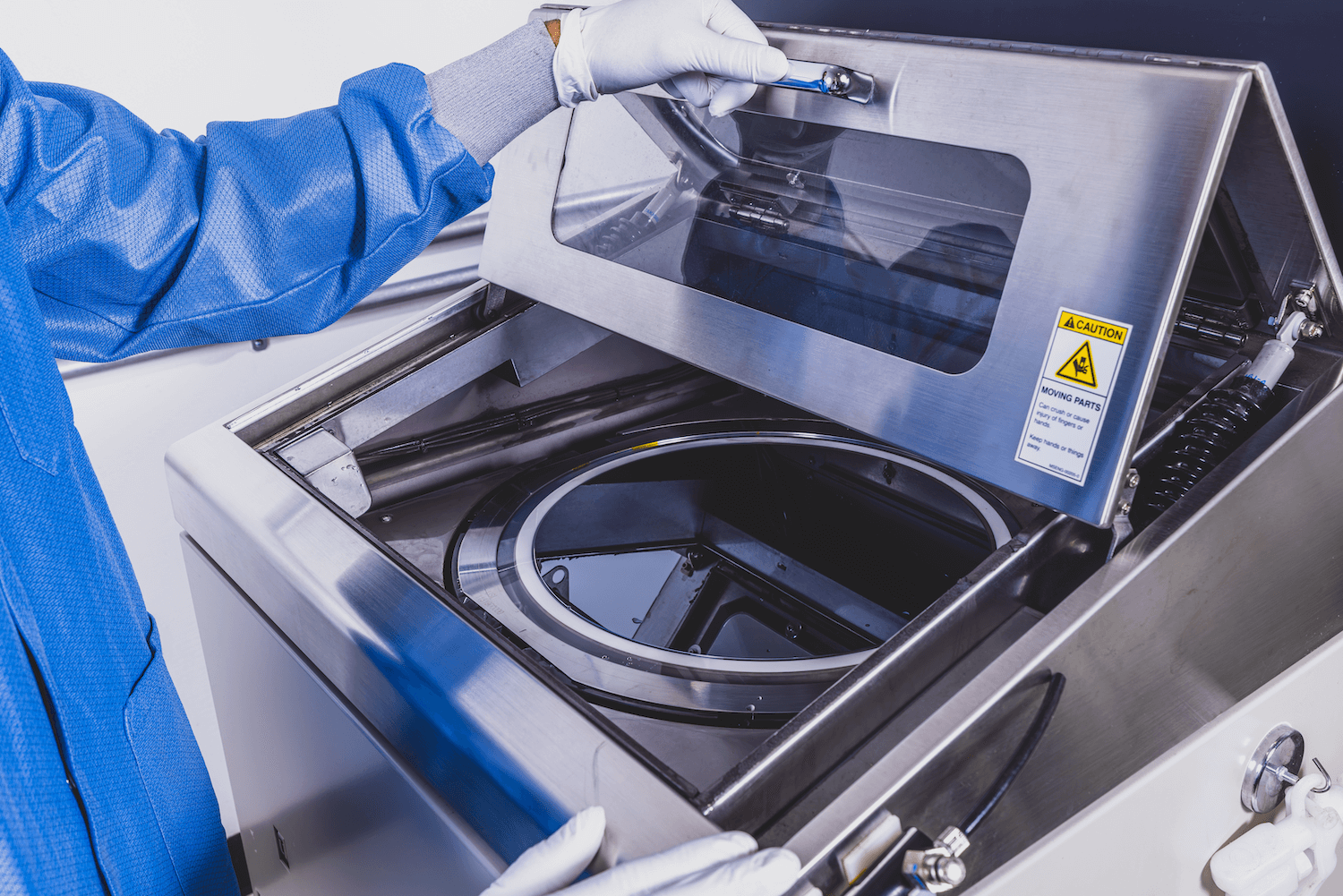
Wafer Dicing
Promex provides high-precision mechanical wafer dicing services using DISCO automated dicing saws, widely regarded as the industry standard for clean, accurate singulation of semiconductor wafers. Our dicing process is optimized to deliver high yield, minimal chipping, and tight dimensional control—essential for preparing dies used in advanced microelectronic packaging.
Mechanical dicing is well-suited for a wide range of substrate materials and device types, including standard silicon wafers, overmolded substrates, and organic laminates.

Key Capabilities:
- Supported wafer sizes: Up to 300 mm
- Dice before grind (DBG)
- Multi-project wafers (MPW), “pizza-mask” wafers and shuttle-run die processing
- Controlled wafer resistivity
- Material types:
- Silicon
- FR4 and other organic/laminate substrates
- Molded plastics and composites
- Glass and ceramic materials
- Stress control: Optimized cut speeds and blade selection to reduce edge chipping and mechanical stress
- Mounting & tape options: Wide variety of UV and non-UV dicing tapes or DAF (Die Attach Film) depending on downstream handling needs
- Thicknesses to 5mm

Die Inspection & Handling
To ensure only known good die proceed to assembly, Promex performs visual and mechanical inspection, sorting, and handling operations using tools optimized for small, fragile components.
- Visual die inspection: Under microscope per industry standards
- Die picking and sorting:
- Automated or manual depending on application
- Individual die traceability to wafer ID or location on-wafer
- Pick per KGD map or sort by die type
- Handling capabilities:
- Thin and ultra-thin dies
- Die attach-ready formats (Gel-Pak, waffle pack, die trays, reconstructed wafers on tape)
- Custom workflows: Configurable processes for customer-specific requirements
Need help calculating how many dies your wafer can produce?
Knowing your die yield can determine factors such as the cost of each die and the scalability of the chip design. Our die per wafer calculator is here to help!
From Wirebonding Inquiry to Full-Scale Production in Genomics
Turning a Sketch into a Production-Ready Module
