
Microelectronics Assembly
Central to Promex’s expertise, semiconductor assembly is a critical stage in the creation of electronic devices, transforming fragile bare dies into robust, functional packages ready for higher-level device integration on circuit boards. The assembly process involves several key steps to establish electrical connection while providing the die with mechanical protection.
Packaged chips are most common; these standalone devices can then be assembled onto circuit boards with traditional surface-mount technology (SMT), enabling broad use. Packaged devices are very robust, offering the highest durability and reliability and enabling device integration into a wide range of applications, from consumer electronics to industrial machinery. This process is essential for the mass production of semiconductor devices, enabling the widespread use of advanced technology in everyday life.
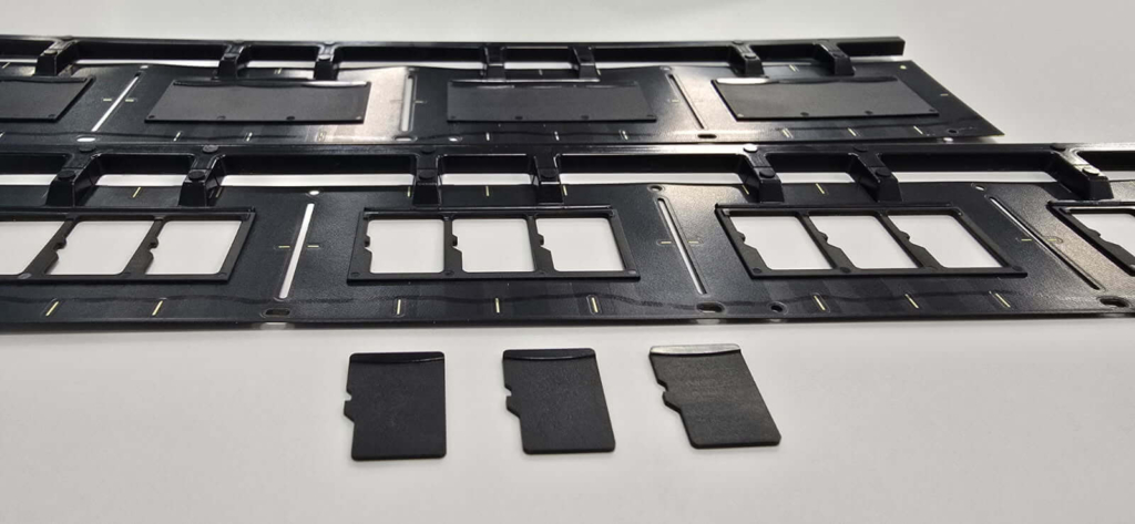
Chip-on-board (COB) offers the advantage of reducing space on the final circuit board (or minimizing space in the Z-dimension), as there is no package. COB requires a customized board for each die device, complicating downstream integration, but can offer improved thermal and electrical performance by mounting the die directly onto a board with minimized interconnect distances. The die and its electrical connections are then protected against mechanical damage with an adhesive through a variety of schemes.
Promex offers a comprehensive suite of turnkey assembly services tailored to support your specialized chip packaging and chip-on-board (COB) applications. Our capabilities include die attach, wire bond, encapsulation, package singulation via laser cutting or mechanical dicing, laser machining, marking and serialization, as well as flip chip technology.
Die Attach
A variety of methods are used to attach the die to a supporting substrate or circuit board. These processes can be performed manually for small batch sizes or automated for higher consistency at volume. Services provided include:
- Epoxy dispense – A variety of materials can be precision-dispensed. Epoxies can be electrically conductive, insulating, and/or thermally conductive. Optical epoxies, silicone materials spanning these functionalities, and thermal greases can also be dispensed with this equipment.
- Underfill – A low-viscosity adhesive doped with non-conductive fillers is injected between die and the substrate, encapsulating areas around bumps forming electrical connection and protecting the assembly from mechanical shock.
- Anisotropic conductive film (ACF)/anisotropic conductive paste (ACP) – Applied as a paste or film adhesive, these materials contain conductive microparticles suspended in a non-conductive matrix. When ACF/ACP is compressed during assembly (by the die mounting surface or under a bump on the die), these particles touch, yielding a conductive path. Areas under the die not subject to compressive forces (typically between interconnect bumps) remain non-conductive. When cured, these materials provide simultaneous conductive adhesion and mechanical support typically accomplished with a separate underfill material.
- Eutectic bonding – Die are placed atop a pre-plated substrate or a solder preform of a eutectic metal alloy, such as 80/20 gold-tin (AuSn) or 88/12 gold-germanium (AuGe). Eutectic bonds employ materials with high mechanical durability and high thermal conductivity within a very thin (~ 5 µm) bondline, making them ideal for high-power and high-reliability devices.
- Solder paste – Traditional solder materials and fluxes are combined in a paste that is printed through openings in a flexible stencil using an automated squeegee. Pastes can have a variety of particle sizes, flux, and solder compositions.
- Sintered silver – Pastes dispensed like a traditional die attach epoxy, these materials are cured at high temperatures under controlled conditions, sintering silver particles and producing unmatched thermal conductivity (70 W/m-K or greater) and good mechanical strength. Sintered silver is excellent for power device assembly. Die-attached film (DAF) – A thin adhesive film used in microelectronic assembly to bond semiconductor chips onto substrates. It enhances precision, reliability, and thermal management in intricate electronic components. DAF is applied to the back of a wafer before saw singulation (DAF is not used with laser singulations). During sawing, the wafer and adhesive DAF layers are cut, resulting in a die with a perfectly sized piece of die attach material on each die. DAF also produces superior bondline thickness consistency without risks of internal voids—especially important for high-power applications.
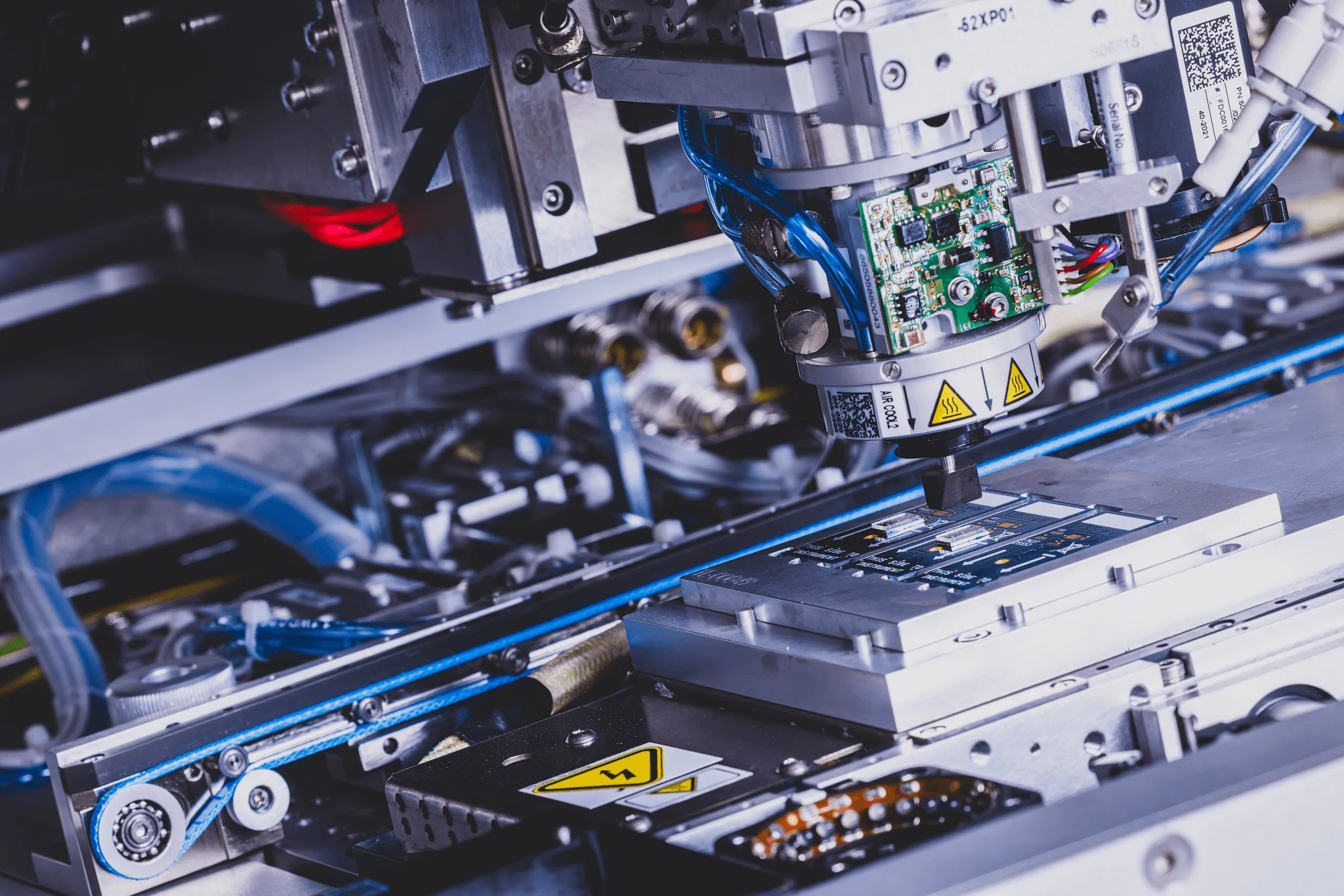
Wire Bonding
Wire bonding is used to create electrical interconnections between a semiconductor or IC and its packaging using fine bonding wires made of materials such as gold and aluminum. Wire bonding processes that Promex offers include:
- Gold with ball bonding
- Aluminum or gold wire with wedge bonding
- Gold or aluminum ribbon with wedge bonding – ribbon sizes 1.4 x 0.25 mil to 10 x 1 mil (35 x 6 µm to 250 x 25 µm)
- Gold wire – wire diameter 0.6 to 2.0 mils (15 to 50 µm)
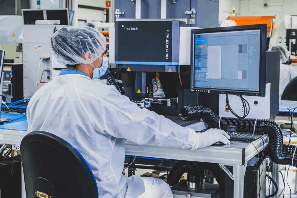
Promex offers a full suite of wire bonding capabilities to support complex microelectronic packaging requirements. Our equipment includes the fully automatic Hesse BJ855 ribbon bonder, the K&S IConn Plus ball bonder for high-speed fine wire applications, and semi-automatic Westbond 4KE systems for process flexibility. We support both fine wire and ribbon bonding using gold and aluminum, enabling solutions for a wide range of high-reliability applications—including medical devices, aerospace, defense, and advanced semiconductor packaging. Our wire bonding capabilities are engineered for precision, versatility, and dependable performance in demanding environments.
Encapsulation
Encapsulation shields delicate microelectronic components when deployed in their applications. It ensures protection against environmental factors, ensuring reliability, safety, and long-term functionality in sensitive devices. For devices requiring subsequent surface mount assembly, encapsulation enables handling with traditional pick and place equipment.
Dam and fill – A dam is formed by dispensing a perimeter of low-viscosity adhesive around wirebonded die and filled with a low-viscosity adhesive to protect die and wires. Alternatively, a pre-fabricated frame can be adhered to the substrate to form a dam prior to filling. The dam and fill encapsulant can be lapped to a controlled height, if desired.
Air cavity / lid – A specialized package type that is pre-molded around a conductive leadframe, forming a cavity for subsequent assembly. Air cavity packages offer simplified assembly in a variety of standard packages.
Overmold – Dies are adhered and wirebonded to a leadframe array strip before being overmolded with a thermoset material designed for microchip packaging. Mechanical sawing is then employed to singulate finished devices.
Microfluidic options – Promex can develop custom processes to either pattern or bond non-electronic parts to create sealed microfluidic channels atop a bare die surface. Processes can be developed to preserve delicate surface chemistries, if desired.
Promex features a GPD Global Max II automated dispense/jetting system, multiple Datacon Evo 2200+ systems that combine automated dispense and precision pick and place (3σ accuracy +/- 7µm), and a Datacon Evo 2200 system (3σ accuracy +/- 10µm). Our skilled operators can also perform complex manual dispense operations, if desired.
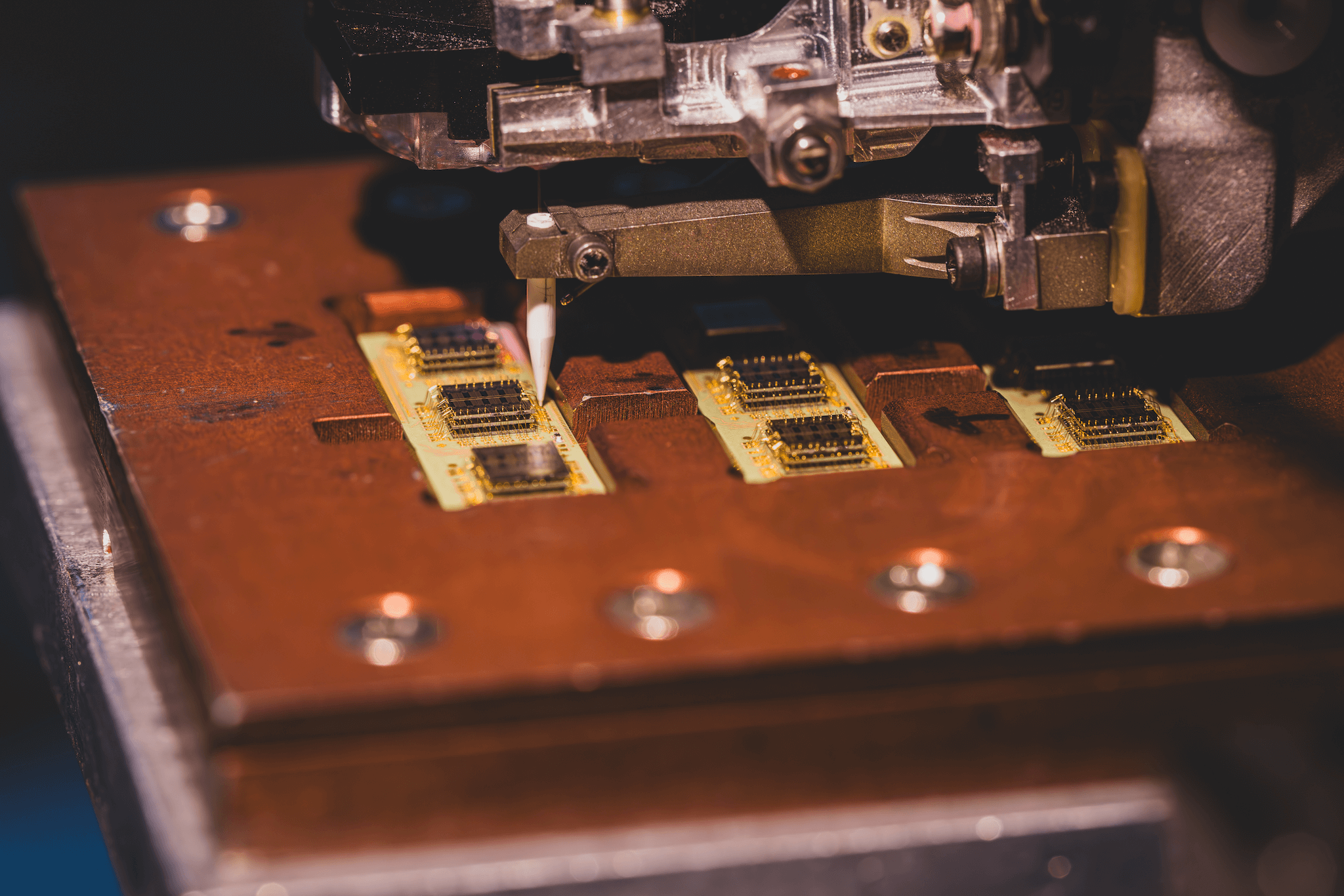
Package Singulation
Singulation is the process of separating arrays of interconnected microelectronic components into individual parts. Singulated parts can then be handled with traditional assembly equipment, such as pick and place for surface mount assembly.
Promex offers mechanical saw singulation with several dicing saws. We feature state of the art, fully automatic dicing systems from Disco. Our saws are modified to have high exposure, enabling singulation of packages up to 5 mm thick comprised of a variety of materials, such as metal, epoxies, mold compounds, glass, plastic, and others. We can singulate arrays to 12-inch (300 mm) diameter.
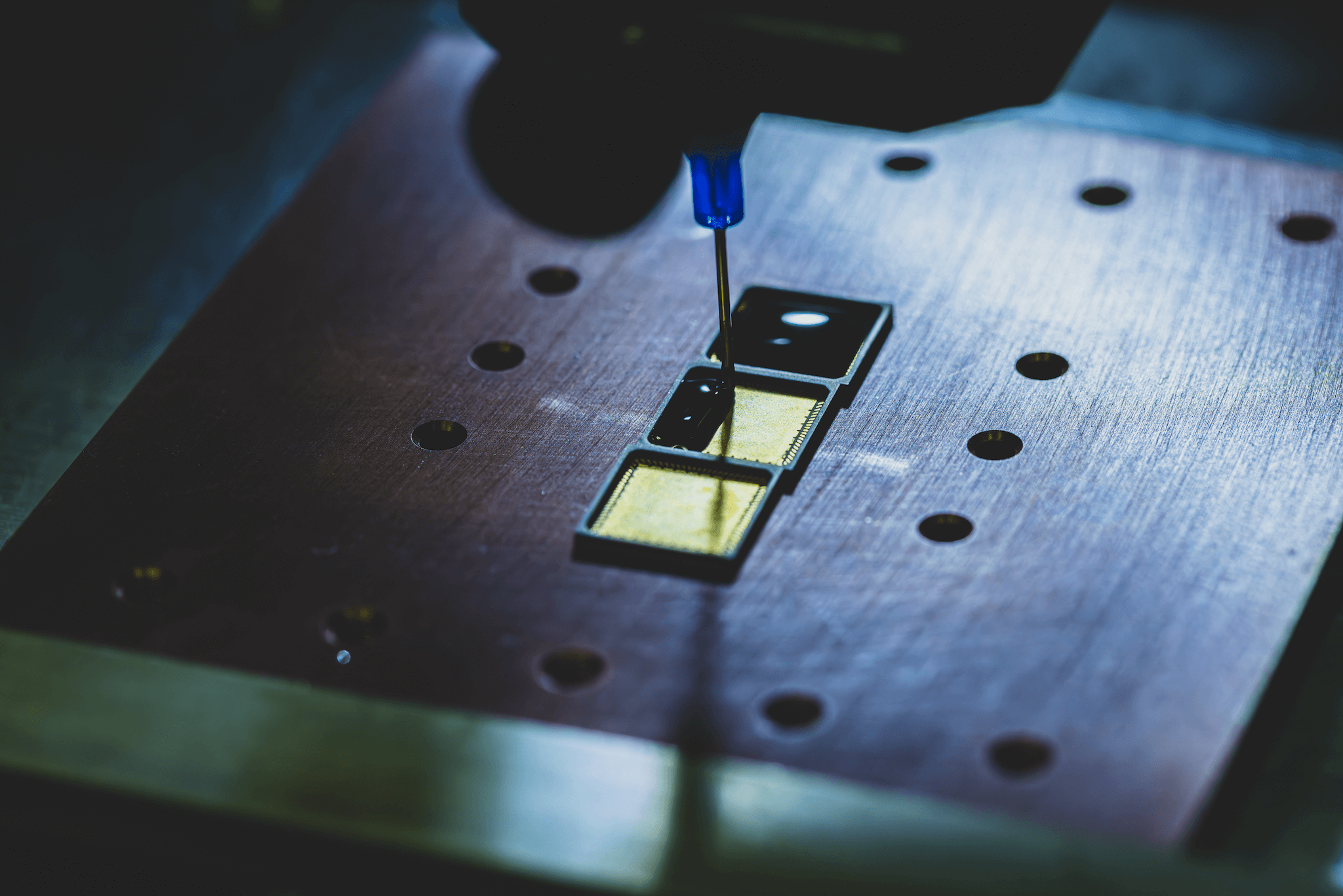
Promex also offers laser singulation using our LPKF CuttingMaster 2127 system. This laser offers a small spot size (<20 µm), operating with 15 ns pulses at ultraviolet wavelengths (355 nm). Custom processes can be developed to singulate a variety of package designs and configurations, including non-rectangular devices.
Laser Singulation and Laser Machining
Promex also has multiple in-house tools to perform laser singulation, micromachining, and cutting for a wide range of materials required for microelectronics and heterogenous integration. Our skilled staff can help you turn an idea into a reality, either as a standalone service or combined with other assembly services, simplifying your supply chain.
Laser depaneling uses a focused laser beam to separate individual PCBs from a larger panel after manufacturing. Widely used in PCB manufacturing, flex circuit depaneling, and rigid-flex board processing, the highly precise process minimizes dust and mechanical stress.
We feature an LPKF CuttingMaster 2127 (27W, 355 nm, 15 ns pulse) laser with a spot size of <20 µm. This laser is ideal for cleanly and quickly cutting organic materials without melting, charring, or thermal stress, such as:
- FR4 circuit boards
- Polyimide flex boards
- Liquid crystal polymer (LCP) flex boards
- Organic/laminate substrates and interposers
- Overmolded components and other plastics/composites
With this tool, we offer the following prototype and volume production services:
- Circuit board depanelization (max. panel; thickness up to 2.0 mm)
- Maximum panel size: 350 mm x 350 mm
- Thickness range: Up to 1.6 mm (thicker upon request)
- Positional accuracy +/- 25 µm
- Allowed components within 30 µm of PCB edge possible
- Panelization layout design – can accommodate both AutoCAD (.dxf or .dwg) and Gerber (.gbr) files
- Save up to 30% dead space between devices on panel due to small laser spot size
- Laser drilling
- Laser circuit rework (trace cutting, solder mask removal)
Board or device serialization- 1D or 2D barcodes (data matrix, QR codes)
- Numerical serialization
- Logos or other artwork
- Process development and material cutting feasibility studies
Enabling clean, stress-free singulation of flex and rigid-flex circuits is key to meeting customer demand for chip-on-flex and flexible packaging solutions. Offering this capability in-house allows Promex to improve turnaround times, enhance process control, and ensure consistent quality for critical applications.
Laser machining is a broader term that encompasses various laser-based material processing techniques. For other micromachining services, we have an ESI 5220 Laser Processing System that allows us to process:
- Glass and other optical materials, including sapphire
- Ceramics
- Silicon, including wafers
- Metals, including copper, nitinol, and stainless steel
Laser micromachining with this tool can accommodate parts up to 533 mm x 635 mm in size (thickness is material dependent), enabling:
- Silicon wafer coring from wafers up to 300 mm custom extraction of smaller development wafers
- Drill micro-vias as small as 25 µm in diameter
- Cut grooves, steps, channels, slots or cavities
- Inscribe alphanumeric characters, logos, or alignment features
- Trim, drill and dice MEMS devices
- Drill precision alignment holes
- Laser-cut stencils
- Cutting and depanelization
Promex can also rework substrates by laser cutting surface-layer traces and removing excess solder mask. Let us review your requirements!
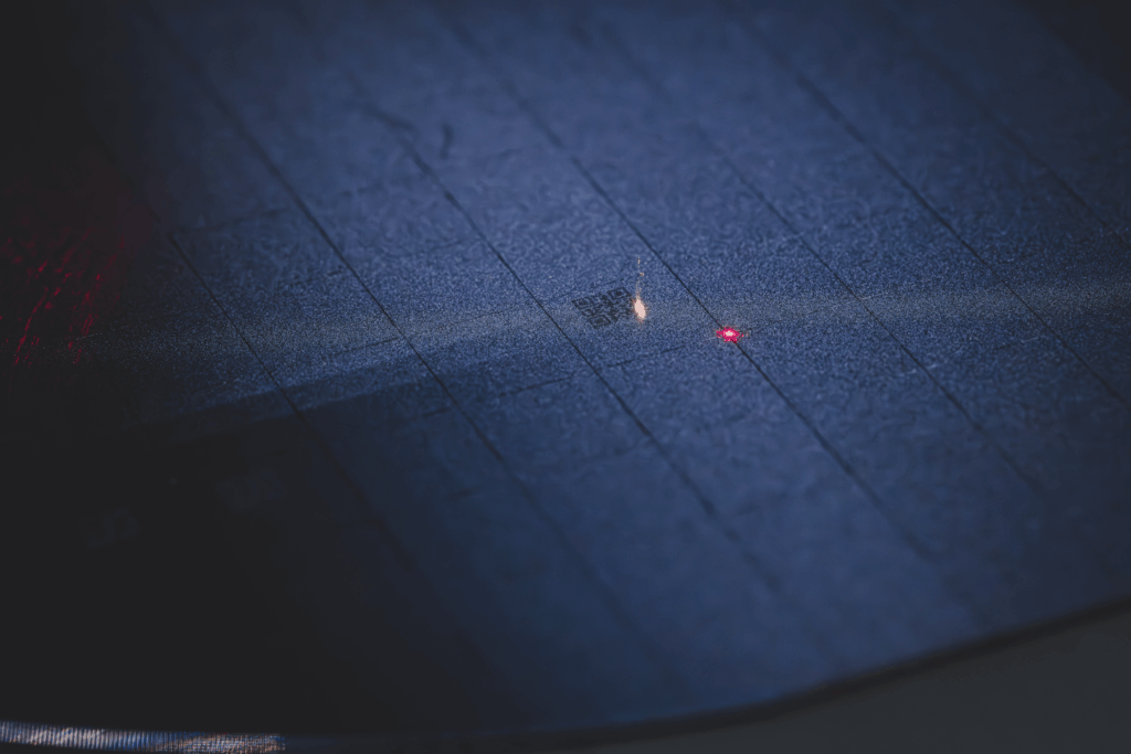
Laser Marking & Serialization
Laser marking employs focused beams to engrave human- or machine-readable codes, patterns (such as barcodes and QR codes), or custom artwork, including company logos, on microelectronic components for quality control or for corporate branding. Marking per your requirements ensures part- or lot-traceability for quality control and compliance. Marking can be performed on a variety of materials and locations, including:
- Bare die
- Metal, ceramic, glass, or plastic lids
- PCB surfaces
- Packaged microchips
- Other passive components
Flip Chip Technology
Flip chip technology involves mounting semiconductor chips face-down, or active-side down onto organic or ceramic circuit boards using conductive bumps on the chip bond pads. This process, which improves electrical connections and space efficiency to enhance performance and miniaturization, is quickly gaining popularity over traditional face-up wire bonding due to its advantages in circuit board real-estate reductions, performance, reliability, and cost over other packaging methods. Flip chip assembly services are essential for such microelectronic device applications as µBGA, 3D packaging, optoelectronic bonding and assembly, sensors, chip-on-glass, and more.
- Our flip chip services include:
- Flip chip bonding: Bonding that uses a solder bump, Cu pillar, or Au stud bump
- Thermosonic bonding: A technique that uses ultrasonic energy and heat to create a bond
- Thermocompression bonding: A method that applies heat and pressure to form a bond
- ACA (anisotropic conductive adhesive): A type of adhesive that conducts electricity in one direction
- NCA (non-conductive adhesive): An adhesive that does not conduct electricity
Why choose Promex for flip chip technology?
- Expertise: Our team has extensive flip chip technology experience, ensuring high-quality and reliable assembly
- Customization: We offer tailored solutions to meet the specific needs of your microelectronic applications
- State-of-the-art facilities: Our advanced facilities are equipped with the latest technology to handle complex flip chip assemblies
- Quality assurance: We adhere to strict quality control standards to ensure the best performance and reliability of your products
From Wirebonding Inquiry to Full-Scale Production in Genomics
Turning a Sketch into a Production-Ready Module
