Our Capabilities

Our Capabilities

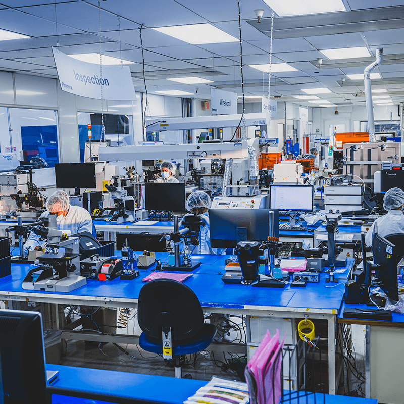
Promex, located in Silicon Valley, is your all-in-one solution for complex assembly of devices that have semiconductor die and/or non-electronic parts. Tired of the complexities of working with different facilities for various process steps? We’ve streamlined it all under one roof, certified ISO 13485 with Class-100 and Class-1000 cleanrooms.

SMT, Wafer Prep, Die-Attach & More

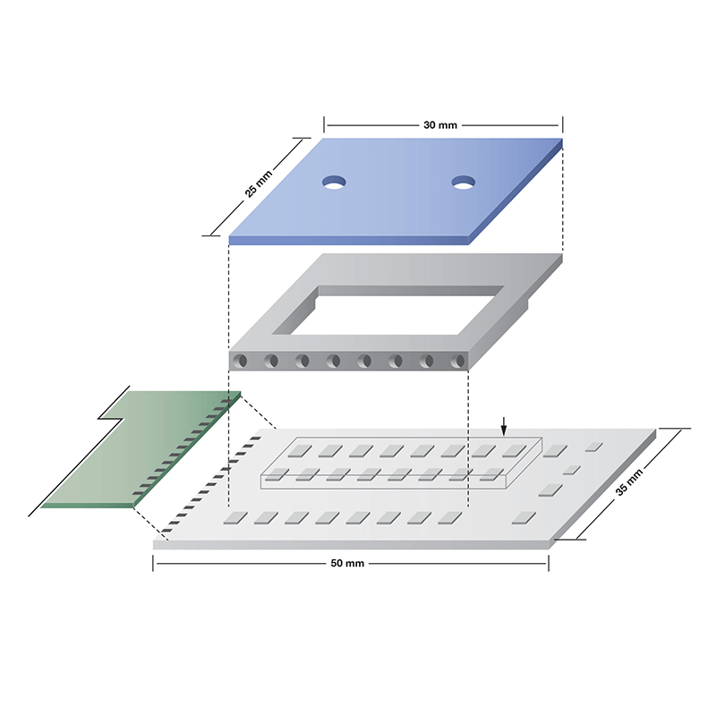
From SMT to wafer prep, die-attach, wire bonding, flip chip, encapsulation, and singulation, we’ve got you covered. At Promex, we’re experts in tackling complex assembly challenges for a wide array of applications, including semiconductors, optics, diagnostics, life sciences, medical, and MEMS devices.

Our innovative process flows seamlessly integrate electrical and non-electrical components into unique micro-assemblies. We excel in heterogeneous integration of tiny components with custom requirements, ensuring your project’s success.

Our Capabilities

Click On A Capability To Learn More

Surface Mount Technology (SMT)

Assembly

Die Prep

Wafer Processing

Substrate Design & Fabrication

Metrology

Process Development

Project Management

Surface Mount Technology (SMT)

Assembly

Die Prep

Wafer Processing

Substrate Design & Fabrication

Metrology

Process Development

Project Management

Subassembly Using SMT Processes

Subassembly Using SMT Processes

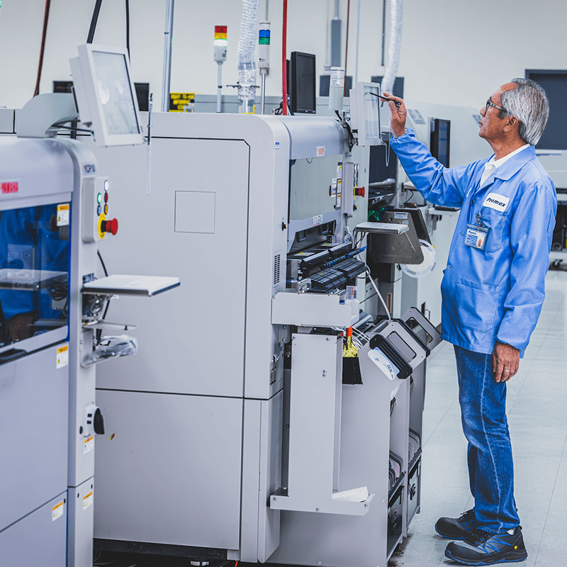
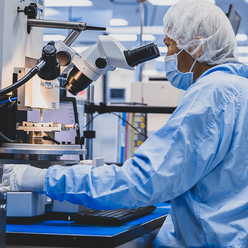
promex employee working on an SMT subassembly machine
Subassembly Using SMT Processes

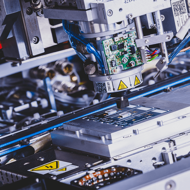
Our SMT subassembly process begins with the substrate, followed by solder dispensing, part placement, solder reflow, cleaning, and inspection. Collaborating with you, we select the best materials and processes for each step, ensuring precision and quality. We have some of the most experienced SMT operators in Silicon Valley and can guarantee extremely high quality for the most challenging projects and needs.

Wafer Processing Through Encapsulation

Our wafer processing capabilities include backgrinding, die-attach film (DAF) application, sawing/singulation, and precision die attach with epoxy curing or flip chip reflow. We follow up with plasma cleaning, wire bonding, and encapsulation, ready for further special processing as required.

Specialized Part Placement and Attachment

Whether your device needs to incorporate fluid seals, optical filters, image sensors, or MEMS, we handle specialized parts with tailored processes. Your project moves seamlessly from specialized part placement to final testing, ensuring a efficient path to market success.

Surface Mount Technology (SMT)

SMT is the assembly method for placing and soldering microelectronic components onto PCBs or other substrates. It optimizes space, speed, and precision, enabling advanced functionality and integration.

    • 2 full SMT Lines
    • Flexible and Rigid-flex
    • 008004 and Larger Parts
    • Chip On Board (CUB)
    • Variety of Solder
    • Variety of Reflow Methods

SMT Assembly Services

    • Solder Stenciling and Chip Shooting
    • Nitrogen Reflow
    • Vacuum Reflow
    • Ball Attach
    • Flexible and Rigid-flex
    • “Odd” Form Factor
    • 008004 and Smaller Parts
    • Chip Scale Packages (CSPs)
    • Singulation of Panelized Parts

Specialized Assembly

Specialized Assembly

wirebond machine up close

Specialized Assembly Services

Die Attach

Die Attached Film (DAF) is a thin adhesive film used in microelectronic assembly to bond semiconductor chips onto substrates. It enhances precision, reliability, and thermal management in intricate electronic components. The film is applied to the back of a wafer before saw singulation (DAF is not used with laser singulations). During sawing, the wafer and adhesive DAF layers are cut, resulting in a die with a perfectly sized piece of die attach material on each die.

Wire Bond
    • Gold Ball
    • Aluminum Wedge
    • Ribbon
    • Au Wire, 0.6 to 2.0 mils


Encapsulation

Encapsulation shields delicate microelectronic components in applications. It ensures protection against environmental factors, ensuring reliability, safety, and long-term functionality in sensitive devices.

    • Dam and Fill
    • Air Cavity / Lid
    • Over Mold
    • Microfluidic Options
Package Singulation

Singulation is the process of separating interconnected microelectronic components into individual parts. It ensures individual functionality and seamless integration for optimal performance and reliability.

Laser Marking & Serialization

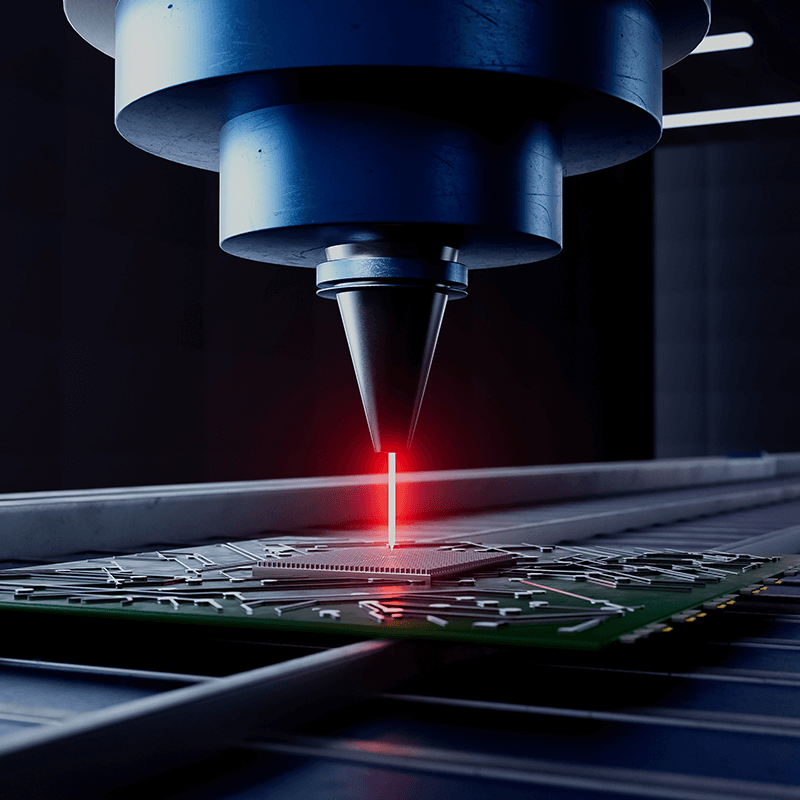
Laser marking employs focused beams to engrave codes or patterns on microelectronic components for a variety of purposes. It ensures traceability, authentication, and durability for quality control and compliance.

    • Flip Chip
    • Thermo Compression Bonding (TCB)
    • Underfill
    • Epoxy Lid Attach
Epoxy Dispense

Epoxy dispense involves accurately applying adhesive material onto microelectronic components in medical devices or biotech devices. This ensures secure bonding, thermal management, and protection from the environment to ensure reliable functionality in demanding applications.

Die Preparation

Die Preparation

encapsulation

Die Preparation Assembly Services

    • Backgrind
    • Die Attach Film (DAF)
    • Epoxy Dispense
    • Die Attach
      • ACF/ACP
Flip Chip Technology

Flip chip technology involves mounting semiconductor chips active-side down, improving electrical connections and space efficiency to enhance performance and miniaturization.

Wafer Processing

Wafer Processing

close up of wafer lamination
Wafer Processing

Involves intricate steps like etching, deposition, and lithography to create microelectronic components for medical devices and biotechnology tools. It ensures precision, performance, and reliability in critical applications.

Wafer Dicing

Wafer dicing is the process of cutting a semiconductor wafer into individual chips. It’s integral to microelectronic assembly, enabling precise creation of components for various devices, from smartphones to sensors. Promex has some of the most experienced wafer dicing operators in the nation and can work with you to take on your most challenging projects and needs.

Wafer Backgrinding

Wafer backgrinding involves thinning a semiconductor wafer’s backside to enhance flexibility and reduce thickness. It’s crucial for producing ultra-thin chips in intricate microelectronic assembly, optimizing space and performance.

    • Wafer Backgrinding Down to 30 µm
    • Wafer Dicing
    • Dice Before Grind
    • Die Attach Film (DAF) Expertise
    • Up to 300 mm
    • Multi-project Wafers

Substrate Design & Fabrication

Substrate Design & Fabrication

substrate machine close up
About Our Substrate Services

Promex has long relationships with some of the most trusted partners in the substrate and fabrication market and can help you design, source, and manage fabrication for your custom substrate or interposer.

Metrology

Metrology

Promex employee working on a metrology x-ray machine

In-House Metrology Capabilities

    • Automated X/Y Microscopy
    • Z-axis Optical Profilimetry for Flatness and Surface Roughness Measurement
    • X-Ray Fluorescence to Measure Surface Metallurgy
    • X-Ray Imaging
    • CSAM (Computerized Surface Acoustic Microscopy)
    • Laser Solder Thickness Measurement
    • Hardness Testing of Degree of Cure in Polymers

Process Development

Process Development

flip chip assembly

The Promex Phase Gate Process

At Promex, we support device development from concept through production using our proven phase gate process, which allows you to single-source (turnkey) your complex microelectronic component assembly. We can support everything from short prototype runs, to  pre-production devices, and scale to large-volume production when needed. 

Phase 00: Feasibility

The feasibility phase is to demonstrate that a product concept ‘works’ and can be validated. Test results and/or prototypes are required to close the phase and prove the capability.

Phase 01: Development & Optimization

Processes, materials, and tooling will be developed and selected as part of the development and optimization process. The deliverable is a refined manufacturing procedure with recipes, tooling, and the equipment necessary to fabricate the desired product with a consistency and cost that meets the business needs. This package is suitable for the process validation activities of Phase 02 with minimal, if any, changes. Process Failure Mode and Effects Analysis (PFMEA) is started.

Phase 02: Process Validation

At least three lots are built using the process from Phase 01. All devices meet requirements defined in Phase 01 for the process to be validated. The PFMEA is finalized, and the Process Control Plan is generated. Operational qualification (OQ) and performance qualification (PQ) protocols are written and executed.

Phase 03: Preproduction

Preproduction is a transition state where production-level practices are followed while some of the quality deliverables and documentation are completed. First Article Inspection Report (FAIR) is completed, and reports are submitted to customer for approval.

Phase 04: Production

In this final phase, the processes to fabricate an assembly have been developed, validated, and fully documented to both companies’ satisfaction. The only remaining activity is to accept orders, build product, track yields, and report back to the customer as required.

Project Management

Project Management

exterior shot of Promex headquarters in Silicon Valley
About Our Project Management Services

Document control is the backbone of an effective Quality Management System. The Promex team will work with you to manage all needed documentation during the Phase Gate Process. A benefit of working with Promex is that your complete documentation is managed by one team under one roof, making the process much easier for you.

Promex works with a number of partners to address all testing needs, and you can consign and bring needed customer testing equipment within our facility.

Experience With Multiple Assembly Technologies

To produce miniaturized devices, we combine multiple assembly technologies in a cost-effective way, using rapid process development with minimal time to market. We operate under a sophistitcated manufacturing process known as heterogeneous assembly.

Fully Integrated & Compliant For Assembly

Offering a range of assembly services, from SMT to wafer prep, die bonding, substrates or meteorology —  we’ll help you manage the entire project from start to finish.

Five Decades Of Experience In Miniaturization

Since 1975, Promex has served a variety of clients across the industries of medical & biotech, automotive, military and defense, data and telecom, and more. We operate 30,000 sq-ft ISO13485:2016 certified production facilities, complete with Class 100 / 1000 cleanrooms.

We’ll Be Your Partner

Let Promex help you bring your idea to life. From SMT to assembly, die preparation, wafer processing, and more, we’ll provide the manufacturing services you need to build your technology.

Ready To Get Started?