Semiconductor Electronic Manufacturing Services
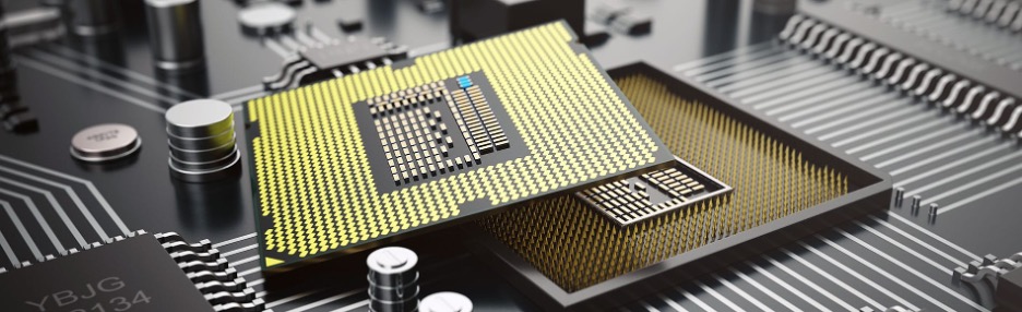
Semiconductors are the foundation of modern electronics, enabling the functionality of everything from smartphones and laptops to automobiles and industrial machinery. These materials have electrical properties that can be precisely controlled, making them essential for creating transistors, diodes, and integrated circuits. As the world becomes increasingly digital and connected, the demand for faster, smaller, and more energy-efficient semiconductor devices continues to grow, driving relentless innovation across the industry.
Miniaturized components, including transistors and integrated circuits, form the basis of semiconductor devices. They enable the control and amplification of electrical signals, supporting the functionality of microchips in computers, smartphones, and countless other electronic devices. Microelectronics ensure the reliability and performance of semiconductor technology, underpinning advancements in computing, communication, and electronics across the globe.
Market Trends
From advanced AI systems and 5G communications to electric vehicles and the Internet of Things (IoT), demand for higher performance, lower power consumption, and greater device functionality is driving ongoing semiconductor innovation. While semiconductors have traditionally been built using silicon, compound semiconductor devices fabricated from III-V material combinations, such as silicon carbide (SiC) and gallium nitride (GaN), have gained a foothold in markets that require the benefits their wide-bandgap structure affords. This includes
One of the most significant trends reshaping the semiconductor landscape is the industry’s shift toward heterogeneous integration. Rather than relying solely on monolithic scaling to improve performance, manufacturers are increasingly turning to multi-die solutions that combine different technologies—logic, memory, sensors, RF, photonics—into a single package. This approach offers clear advantages in flexibility and performance but also introduces new challenges in thermal management, signal integrity, and overall assembly complexity.
Chiplet-based design strategies are another major factor influencing packaging requirements. By breaking large chips into smaller, functional chiplets that can be manufactured separately and assembled later, companies can improve yields, reduce costs, and mix-and-match the best process technologies for different functions.
Challenges
These demands are placing unprecedented pressure on packaging technologies, which must not only keep pace with silicon advancements but must also enable more complex integration approaches, tighter form factors, and improved reliability. Package architectures such as 2.5D interposers, fan-out wafer-level packaging (FOWLP), and system-in-package (SiP) designs are becoming essential to meet these integration goals. And assembling chiplets into a cohesive package, often with very fine pitches and tight alignment tolerances, stretches the limits of traditional packaging and substrate capabilities. It also raises the stakes for ensuring high-bandwidth, low-latency connections between chiplets, making the choice of interposers, advanced substrates, and options such as hybrid bonding critical.
Solutions
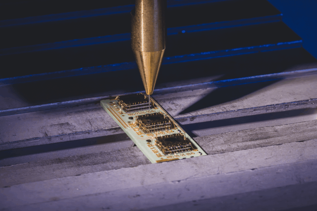
Promex specializes in advanced semiconductor packaging and assembly services, delivering high-reliability solutions for medtech, biotech, aerospace, defense, and other advanced applications. We bring together decades of experience and a broad range of capabilities to support customers at every stage of development, from early prototypes to low- and medium-volume production. Our services include chip-on-board assembly, system-in-package integration, surface-mount technology (SMT), a full range of die and wafer pre capabilities, and substrate packaging design and development, leveraging our expertise in heterogeneous assembly and packaging all types of delicate devices.
We offer die attach, wire bonding, flip chip assembly, overmolding, and precision PCB assembly, all performed in our ISO 13485-certified facilities with cleanroom environments to meet the stringent requirements of medical and mission-critical devices. Our quick-turn prototyping services help accelerate time to market, while our custom process development ensures that each project receives the specialized attention it needs. We also provide wafer dicing, device singulation, and failure analysis support to help customers refine and optimize their designs. At Promex, we are committed to delivering high-quality, flexible manufacturing solutions that help bring your most innovative ideas to life.
